BGA Packaging Pin Evolution and Basic Fan-Out Strategy
In the world of modern high-density interconnect circuit board design, BGA PCB design is undoubtedly the ultimate watershed moment testing an engineer’s skills. Traditional chip pins, like the legs of a centipede, are neatly arranged around the chip (e.g., in QFP packaging). We can see and touch them, and routing simply involves pulling leads from the edges. However, as chip functionality increases and the number of pins surges from dozens to hundreds or even thousands, the edge space around the chip becomes insufficient.
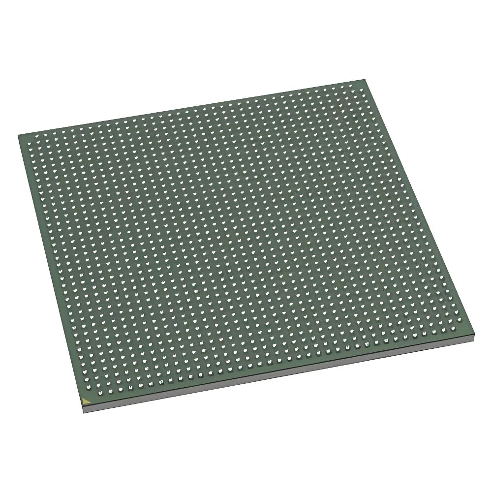
Thus, Ball Grid Array (BGA) packaging was born. It breaks the limitations of “around arrangement,” directly making the pins into tiny solder balls, densely packed like a chessboard on the bottom of the chip.
While this revolution exponentially increased chip integration, it also brought unprecedented three-dimensional geometric challenges to circuit board routing: how to safely connect the large number of pins enclosed at the core and innermost part of the circuit board to external circuits? This is the “fan-out” battle we must face.
The “Step-by-Step” Difficulty Classification of Array Pitch To win this routing battle, we must first understand the enemy’s layout—that is, the center-to-center distance between BGA solder balls (known in the industry as pitch). This distance directly determines the manufacturing difficulty and production cost of the entire circuit board.
In practical engineering, we usually divide the pitch into two hard camps. The first is the standard BGA with a pitch of 0.8 mm and above. This size is very friendly to traditional circuit board manufacturing processes. Because the pitch is relatively loose, we can use ordinary mechanical drilling on ordinary multilayer boards to squeeze one or even two signal lines between the two solder balls. This is the limit of traditional processes, and the cost is very controllable.
The second camp is the micro BGA of 0.4 mm to 0.5 mm (common in smartphone chips or high-end high-bandwidth memory). Once we enter this field, traditional processes are completely paralyzed. Because the physical distance between the two solder balls is too close, even the finest traditional mechanical drill bit will directly shred the adjacent pads when drilling. At this point, the design must be upgraded to HDI (High-Density Interconnect) technology, using precise lasers to burn in microvias, resulting in a qualitative leap in wiring technology.
The classic “dog-bone fanout”: a perennial favorite of traditional processes.
For BGA chips with a pitch of 0.8 mm or more, engineers commonly use a wiring technique called “dog-bone fanout.” If you look vertically down from above the circuit board, you’ll see how vivid this design is.
Its standard construction is as follows: for each circular pad of the BGA, an extremely short, extremely thin lead is pulled outwards, and then a via is punched at the end of the lead to connect to the conductor. The combination of the circular pad, the short lead, and the circular via visually resembles a small dog bone.
Why go to the trouble of creating a “dog-bone” structure instead of simply punching the hole in the center of the pad? Behind this lies the physics of “capillary action” and the painful lessons learned from poor soldering yield.
If we leave vias directly in the center of the pads during assembly, the solder paste will melt and become liquid when the circuit board enters the 260°C high-temperature reflow oven. According to the principle of liquid flow, this liquid solder will flow directly down the walls of the vias to the back of the circuit board or into the inner layers. This is similar to water flowing downhill, resulting in insufficient solder remaining on the surface, leading to “cold solder joints” or “open solder joints” between the chip pins and the circuit board. The product may be scrapped immediately after leaving the factory due to poor contact.
The “dog bone” design perfectly solves this problem. The extremely short lead acts like a bridge, and a layer of green solder resist (green solder mask) covers the lead surface. The green solder mask acts like a gate; it doesn’t stick to solder and effectively confines the molten solder paste within the circular pads, preventing it from flowing into the vias. In this way, signal transmission to the inner layers is achieved while ensuring a stable soldering process during assembly.
Via-in-Pad Technology: The Ultimate Choice Under Space Limits
However, as chip integration density continues to soar, reaching the point of miniature BGAs with pitches of 0.5 mm or even smaller, the “dog bone” process reaches a dead end. In such a small space, even fitting a single pad is cramped; there’s simply no extra space to run the lead and create a separate via.
At this point, engineers must break with convention and adopt a desperate measure—the via-in-pad. As the name suggests, it disregards the risk of solder paste leakage and places the conductive via directly in the center of the BGA’s circular pad.
To solve the aforementioned fatal flaw of “solder paste leaking through the hole,” PCB manufacturers must introduce two extremely expensive additional special processes during PCB fabrication: resin plugging and point-of-freedom (POFV) plating.
After the PCB manufacturer drills the hole in the center of the pad and completes the metallization and conductivity, a special epoxy resin (insulating adhesive) must be used to completely fill and seal the hole, leaving no gaps. Then, mechanical equipment is used to smooth out any excess resin protruding from the surface. Finally, a smooth layer of copper is electroplated onto the resin-filled pad surface.
After these two high-precision processes, the pad appears as a perfect, solid, mirror-finish copper sheet with extremely high flatness. When the automated placement machine places the chip on it for soldering, the molten solder paste finds that the surface is solid, with no holes to allow it to penetrate, thus completely eliminating the risk of cold solder joints. While through-hole designs save engineers significant wiring space and reduce the number of layers in multilayer boards, the processing cost of the PCB increases significantly due to the “resin filling + surface smoothing + secondary electroplating” process. This is the technological premium that must be paid to achieve the ultimate in size.
The Art of Escape Routing
Once we’ve completed the fan-out design of the BGA’s external pads, the real challenge begins. Faced with a high-end chip with thousands of pins, how do we safely and systematically “escort” the densely packed, heavily surrounded internal pin signals to the external routing area?
In the industry, this visually striking process is known as “escape routing.” If we compare a BGA package to a heavily fortified circular castle, then signal escape is a “breach of the siege” operation from the outside in. Engineers can’t just haphazardly run and route the traces; otherwise, the outer rings would become impenetrable walls, trapping the signals in the inner rings. To solve this space challenge, we need to employ an effective tactic—layer stripping.
The Three-Dimensional Layering Logic of Layer Stripping
The core idea of the stripping tactic is simple: fully utilize the vertical space of the circuit board, allowing different signals to “travel through different layers.”
First Layer (Outermost Line of Defense): When we begin routing on the top layer of the circuit board, the first and second rows of pads on the outermost ring of the BGA are very easy to handle. This is because they are right next to the edge of the “castle,” with no external obstructions. Engineers can directly run traces on the surface layer, spreading them outwards. These two rings of signals do not require any vias and can “escape” directly on the surface layer.
Second Layer (Inward Push): When dealing with the third and fourth rows of pads, since the surface layer is already filled with traces from the outer ring, signals cannot be directly pulled out from the surface layer. At this point, we need to use the “dog bone” or “via in pad” technique mentioned in Chapter 1 to create vias at the third and fourth rows of pads, allowing the signals to descend vertically to the first inner signal layer of the circuit board.
Upon reaching this inner layer, the corresponding positions of the outer ring are empty (because the outer ring signals were routed on the surface layer), allowing the signals of the third and fourth rows to be easily pulled outwards from this inner layer. Deep Water Zone (Core Power and Ground): Similarly, signals in the fifth and sixth rows require vias to descend deeper into the inner layers before they can be routed. The pins enclosed in the core, the central area, are typically the chip’s power and ground pins.
These pins don’t need to extend far outwards; during the via descent, they are “intercepted” midway and connected to dedicated inner-layer power or ground planes on the circuit board. Through this outward-to-inward, layer-by-layer, and ring-by-ring design, we can perfectly distribute congestion and conflicts that cannot be resolved on a single plane across the various “layers” of the circuit board.
Layer Number Planning: Many clients, at the beginning of a project, are most concerned with: “My chip has so many pins, how many layers do you need for your BGA PCB design? More layers are too expensive, fewer layers won’t allow for routing?” Assessing the number of layers isn’t a matter of guesswork; there’s a straightforward, industry-standard calculation logic: look at the number of pin rows on the deepest side of the BGA.
Suppose a large BGA chip is a 20×20 square array with 10 rows of pads from the outermost ring to the core. Following the previously mentioned stripping rule of “one signal layer for every two rows of pads”: the top layer handles rows 1 and 2; inner layer 1 handles rows 3 and 4; inner layer 2 handles rows 5 and 6; inner layer 3 handles rows 7 and 8; and inner layer 4 handles rows 9 and 10. This means that just to bring out these 10 rows of signal pins, we need at least 5 dedicated signal routing layers.
In actual layer stack-up designs, to ensure PCB symmetry and prevent warping, and to insert necessary power and ground layers for shielding between signal layers, the total number of layers on the board can easily reach 10 or 12. If a customer, in an effort to save money, insists on craming a BGA that requires a 12-layer board into an 8-layer board, the result will be a severe shortage of routing channels on the inner layers. To force the traces through, some engineers have to reduce the trace width and spacing to extremely small sizes (e.g., below 3 mils). While this reduces the number of layers, the manufacturing difficulty for the PCB manufacturer increases exponentially, leading to a sharp drop in yield. Ultimately, the “process difficulty fee” charged by the PCB manufacturer may exceed the cost of the saved layers. Therefore, reasonable layer planning involves finding the most economical balance between the PCB manufacturer’s process capabilities and the number of PCB layers.
Impedance Continuity of High-Speed Differential Signals Crossing BGA Arrays
In today’s high-speed digital circuits (such as DDR4/DDR5 memory, PCIe 4.0/5.0 lanes), signal transmission speeds are extremely fast. In this case, traces are no longer ordinary wires but have become “transmission lines.” To high-speed signals, the BGA PCB design area is like a minefield of physical mazes. Signals traversing this array are highly susceptible to impedance discontinuities, leading to signal distortion.
What is this impedance “topographical abrupt change”?
High-speed signals thrive on “flat highways.” In perfect conditions, signal lines emerge from the chip and run within spacious, conventional wiring areas. Due to the uniform electric field distribution, their characteristic impedance can be perfectly maintained at 50 ohms (single-ended) or 100 ohms (differential).
However, when this differential signal line plunges into the BGA array, the situation drastically changes. The once-spacious road is now tightly squeezed in the middle by densely packed metal pads and vertical vias on both sides. These surrounding metal objects generate strong parasitic capacitance. Electrically, this sudden increase in parasitic capacitance directly causes the characteristic impedance of this area to “collapse” instantaneously, potentially plummeting from 100 ohms to 80 ohms.
Such impedance abrupt changes are fatal to high-speed signals. When a signal encounters this impedance cliff during transmission, some energy continues forward, while the rest bounces back like water ripples hitting a wall. This “signal reflection” causes severe overshoot, undershoot, and glitches in the waveform, ultimately leading to data transmission packet loss and frequent blue screens or system crashes.
Solution: Anti-pad Optimization
To prevent high-speed signals from perceiving “terrain changes” when traversing BGAs, advanced routing engineers typically employ two key techniques:
The first technique is called anti-pad optimization. When our vias pass through the inner power or ground planes of a multilayer board, an isolation via must be created on these planes to prevent short circuits between the via and the plane. This area with the via is called the anti-pad. To reduce the huge parasitic capacitance caused by the vias inside the BGA, we intentionally enlarge the size of this anti-pad and “cut off” some of the excess copper around the via. As the copper trace moves further away from the via, the parasitic capacitance naturally decreases, allowing the impedance to return to a normal level close to 100 ohms.
The second technique is called Reference Plane Voiding. On the adjacent ground plane directly below the differential signal lines, the area directly below the BGA array is precisely voided, allowing the signal lines to reference a deeper ground plane. By artificially increasing the vertical distance between the signal lines and the reference ground, the impedance drop caused by space compression can be effectively compensated, ensuring the entire transmission line is smooth and continuous like a mirror from beginning to end.
Power and Ground Integrity (Physical Redemption of Decoupling Capacitors)
In BGA PCB design, if high-speed signal escape is likened to the “troop deployment” of a castle, then power and ground integrity (PI) is the castle’s “logistics supplies.” In very large-scale integrated circuits like FPGAs, GPUs, or main control chips, hundreds of millions of transistors inside will simultaneously turn on or off within nanoseconds during high-speed switching. This extreme transient current demand poses a very stringent challenge to the power supply system of the circuit board.
What are Synchronous Switching Noise (SSN) and Voltage Drop?
When hundreds or thousands of output buffers inside a chip switch states simultaneously, they draw a huge current from the power supply system instantaneously. However, any physical power line and via has inductance. According to electromagnetic principles, the faster the rate of current change, the greater the induced voltage generated by the inductor.
This leads to a fatal consequence: the voltage on the power rails inside the chip will fluctuate violently, producing “power glitches” and “ground bounces.” If the supply voltage drops instantaneously beyond the chip’s allowable baseline (usually ±5% or even lower), the logic gates inside the chip will misinterpret it, mistaking a high level for a low level, resulting in data corruption.
The “Proximity Interception” Principle of Decoupling Capacitors
To smooth out this voltage drop, we must place a large number of decoupling capacitors around the BGA chip. Decoupling capacitors act like miniature “reservoirs,” releasing the stored charge to the chip in the microseconds or even nanoseconds when the main power supply is unable to provide power, thereby stabilizing the voltage.
However, a common mistake made by many junior engineers is that while they may draw dozens of capacitors on the schematic, they neatly arrange them around the BGA chip during PCB layout, leaving them millimeters or even centimeters away from the chip core.
In high-speed applications, this placement is tantamount to “distant water failing to quench immediate thirst.” The long, thin traces and vias between the capacitors and the chip pins introduce inductance, creating a high-impedance bottleneck that effectively blocks current. When the chip needs current, these peripheral capacitors simply cannot deliver it within nanoseconds.
The truly expert placement strategy is simple: place them directly on the back of the BGA (bottom layer).
In multilayer board designs, the center of the BGA is usually filled with power and ground vias. We precisely mount miniature surface-mount capacitors, even those as small as 0201 or 01005, directly and precisely on the back of the BGA chip, directly below it. The capacitor pads are connected directly to the power and ground pins of the BGA chip via the shortest possible vertical vias. This vertical “back-to-back” design minimizes trace inductance, allowing the decoupling capacitors to truly function as “transient power supplies.”
Soldering Mechanical Stress, Thermal Expansion Mismatch, and Warp Control
BGA design is not merely the domain of electrical engineers; it is also a microscopic contest between materials science and mechanical engineering. Since all BGA solder joints are hidden beneath the chip, mechanical breakage during production or customer use is completely undetectable to the naked eye, requiring expensive X-rays or endoscopes for inspection. This poses a significant challenge to long-term reliability.
The “Different Dreams” of Coefficient of Thermal Expansion (CTE)
When the assembled BGA circuit board passes through a 260°C reflow oven, or when the product generates intense heat during operation, both the chip and the circuit board undergo thermal expansion.
Chip Characteristics: Silicon chips (dies) have a very low coefficient of thermal expansion and expand almost nothing when heated.
Circuit Board Characteristics: FR4 or HDI resin substrates have relatively high coefficients of thermal expansion and expand significantly when heated.
This discrepancy in thermal expansion rates causes the tiny solder balls located between the chip and the circuit board to experience intense shear stress. Imagine the board underneath trying to stretch outwards while the chip on top holds it back; the solder balls trapped in the middle are repeatedly kneaded and pulled. During the long-term thermal cycle of power-on heating and power-off cooling, the solder joints at the four corners of the BGA (the most stressed areas) are prone to microscopic fatigue cracks, ultimately leading to cold solder joints or open circuits.
The “Banana Effect” (Warpage) in the Soldering Stage
In BGA PCB design, if the stackup structure is asymmetrical or the copper coverage is uneven, the circuit board will bend in one direction under the high temperatures of reflow soldering, a phenomenon known in the industry as warpage.
If the circuit board bends upwards (like the concave side of a banana), the solder balls in the center of the BGA chip will be squeezed, causing adjacent solder balls to melt and stick together, resulting in a short circuit. Meanwhile, the solder balls at the four corners of the BGA will not touch the pads due to the board’s downward tilt, resulting in empty solder joints.
To completely eliminate warpage during the design phase, IPCB engineers must adhere to strict physical symmetry principles when planning the stackup. That is, with the central geometric plane of the circuit board as the boundary, the dielectric thickness, copper foil thickness, and residual copper ratio (copper density) of the upper half must be a perfect mirror image of the lower half. Only in this way can the tensile forces in all directions cancel each other out under high temperatures, allowing the board to remain flat like a mirror.
Four-Corner Anchoring: Teardrop and Non-Solder Mask Symmetrical Pad Design
To further enhance mechanical strength, we typically employ two process compensation measures during BGA routing:
First, forced teardrop. At the junction of signal lines leading out of BGA pads, the traces are gradually widened, forming a teardrop-like transition structure. This not only smooths signal impedance but also significantly enhances the mechanical tear strength between the pads and traces, preventing traces from breaking off from the pad edges under stress.
Second, NSMD (Non-Solder Mask Limited Pad) selection. In the BGA area, we generally prefer to make the copper foil pads on the circuit board very clean (leaving gaps around the green solder paste), allowing the molten solder paste to cover the entire sidewall of the pad. This increases the contact area between the solder ball and the copper foil, improving the tensile strength of individual solder joints by more than 20%, essentially providing the entire BGA with a layer of protection.