A Macroscopic Glimpse into Microelectronics Physics: Deciphering the Ultra-High-Density Topology of High-Density Mobile Phone Motherboards
In the hardware development landscape of modern smartphones and high-end wearable devices, the smartphone PCB has completely transcended the traditional realm of “printed circuit board” cables. It is essentially a highly complex, ultra-high-density three-dimensional topological skeleton of a microelectronic system, situated between semiconductor integrated circuits (ICs) and traditional rigid substrates.
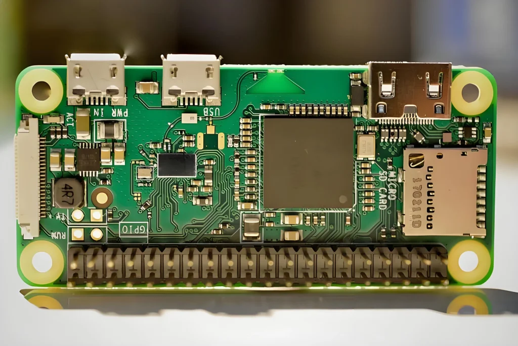
In today’s flagship consumer electronics products that pursue ultimate computing power, ultra-low power consumption, and compressed irregular space, the wiring density of mobile phone motherboards has surpassed the traditional metric of trace length per square millimeter, approaching the micrometer-level physical limits of semiconductor packaging. Line width and line space are relentlessly compressed to the sub-micrometer level, at 1 mil (25.4 micrometers) or even lower. This necessitates a complete revolution in its underlying physical structure, from inorganic materials to micro-manufacturing processes.
High-Density Interconnect (HDI): From Stepped Layering to Anylayer Topological Heterogeneity
Traditional rigid multilayer circuit boards typically rely on through-holes running the entire board. Vertically, this results in a single signal transmission path and significant surface area waste. In extremely thin, highly integrated mobile phone motherboards, the introduction of numerous micro-wafer-level ball grid array (WLCSP) packages and 01005 and 008004-level ultra-miniature resistors and capacitors makes the huge capture pads created by these through-holes a spatial layout killer. To free up insulation space and impedance control bands, modern mobile phone motherboards must fully transition to high-density interconnect (HDI) technology, undergoing a comprehensive topological heterogeneous evolution from first-order (1+N+1), second-order (2+N+2) to anylayer high-density interconnect (Anylayer HDI).
In the heterogeneous topology of Anylayer HDI, the traditional core is completely removed from the overall thickness structure. It is replaced by a coreless stackup composed of multiple layers of ultra-thin polyimide-modified resin (RCC, resin-coated copper foil) or high-density fiberglass microstrips.
The ingenuity of this structure lies in the fact that direct electrical paths can be formed between any two adjacent layers, or even between non-adjacent local layers, from the top layer (Layer 1) to the bottom layer (Layer X), via micro-laser blind vias and buried vias.
This means that circuit routing engineers can completely break free from the vertical physical constraints of vias, allowing differential signal lines that would otherwise require several millimeters to travel to be directly connected within a few micrometers of thickness using vertically stacked blind vias. This not only increases the freedom of 3D wiring several times over, but also significantly shortens the transmission path of high-frequency signals, fundamentally reducing signal attenuation and reflection caused by parasitic capacitance and inductance of vias.
The Hydrodynamic and Electrochemical Mechanisms of Semi-Additive Process (MSAP) in Submicron-Level Linewidth Control
When linewidth and spacing cross the “forbidden zone” below 30 micrometers, the traditional subtractive process—that is, covering the entire copper foil surface with photoresist, exposing and developing it, and then hard etching away the excess copper with acidic or alkaline solutions—completely fails due to irreconcilable hydrodynamic limitations.
In the traditional subtractive process, while the etching solution dissolves the exposed copper foil downwards, it inevitably hollows out the sidewalls of the useful copper lines beneath the photoresist protective film due to capillary effects and uneven chemical diffusion. This is the infamous “under-cut.”
When the original design width of a usable trace is only 25 micrometers, lateral etching of a few micrometers on each side can directly result in a terrifying trapezoidal cross-section with an extremely narrow top and an extremely wide bottom, or even completely ripping the trace off the substrate surface.
To overcome this physical limitation, mass production lines for smartphone PCBs must incorporate the Modified Semi-Additive Process (MSAP).
The MSAP process is, at the microscopic level, a meticulously controlled electrochemical reverse reshaping:
Ultra-thin copper substrate laying:
First, the PCB manufacturer selects an extremely thin initial layer (typically only 1.5 to 3 micrometers) of flash-plated ultra-thin copper foil as the initial seed layer.
Resist-based fine photolithography: On this flash-plated copper surface, a high-resolution dry film or liquid photoresist is imprinted using a high-precision laser direct imaging (LDI) lithography machine, followed by precise exposure and development to completely clear the areas where useful circuits will grow.
Selective pattern plating: The entire substrate is placed in a dedicated acidic copper plating bath. Because the underlying flash-plated copper seed layer is exposed in the microchannels without dry film coverage, copper ions, driven by an external cathode current, selectively grow from bottom to top in these narrow, micrometer-level channels with extreme precision at a rate of several micrometers per minute.
Flash etching: Once the copper plating thickness reaches the design requirements (typically 12 to 15 micrometers), the remaining photoresist film is removed. At this point, the motherboard surface is left with towering useful copper lines and an initial flash-plated copper seed layer only 2 micrometers thick between the two useful copper lines. Finally, the entire board is immersed in a highly selective micro-etching solution (such as a sulfuric acid-hydrogen peroxide system or an ammonium persulfate system) for a very short flash etching process. Because the seed layer between the two lines is extremely thin, it is completely dissolved within seconds, exposing the underlying insulating resin framework. While the towering useful copper lines are also simultaneously micro-etched away by 2 micrometers, their overall structure remains undamaged due to their inherent strength of tens of micrometers.
Through the MSAP process, the rectangular cross-sectional perpendicularity of the useful traces can easily reach over 0.95, resulting in clean, surgically precise edges. This eliminates the disordered ripple transitions in characteristic impedance caused by side etching at the source, ensuring perfect transmission of the ultra-high-speed data bus at the microscopic level.
Electrochemical Kinetic Limits of Microvia Electroplating and the Failure Mechanism of Conductive Anode Wires (CAFs)
In the three-dimensional structure of Anylayer HDI mobile phone motherboards, the millions of laser-drilled blind vias between each layer cannot simply be “hollow vias.” They must be completely solidly closed and filled using high-purity electroplated copper. Only by achieving solid filling can the complex design of stacked vias be realized, allowing the laser center point of the upper layer to directly and unhinderedly strike the top of the solid copper pillar of the lower layer.
Diffusion Restriction and Synergistic Effect of Additives in Microvia Electroplating
From a microscopic electrochemical perspective, completely filling a blind via with copper ions with 60 micrometers in diameter and 40 micrometers in depth is no less difficult than building a seamless solid dam with bricks at the bottom of a turbulent canyon. Inside the electroplating tank, the copper sulfate and sulfuric acid mixture, driven by a strong current, naturally exhibits a much higher electrochemical deposition rate at the orifice edges due to the highly concentrated electric field lines compared to the orifice bottom. If this tendency is allowed to continue unchecked, the copper at the orifice edges will rapidly grow and prematurely close, creating a large void within the blind via.
To counteract this electrochemical tendency, the electroplating tank for smartphone PCBs must incorporate three organic surfactants that work in a balanced, molecular-level equilibrium: a suppressor/carrier, an accelerator/brightener, and a leveling agent.
The suppressor’s physical barrier: Suppressors are typically high-molecular-weight polyethylene glycol (PEG) polymers. During electroplating, their large molecular weight allows them to preferentially adsorb over a large area at the top of the blind via and on flat areas of the board surface where convection in the plating solution is intense. Inhibitor molecules form a dense organic barrier on the copper foil surface, forcibly increasing the local electrochemical overpotential and suppressing the copper deposition rate at the orifice and plate surface.
Microscopic migration of gloss agents: Gloss agents are typically small-molecule sulfur-containing organic compounds, such as bis(3-sulfonyl)disulfide (SPS). Due to their extremely small molecular weight and strong diffusion and migration capabilities, they can penetrate the protective gaps of the inhibitor and flood into the bottom of blind vias, where convection is weak and electrochemical dead zones exist. At the bottom of the via, the gloss agent forms an unstable intermediate complex with copper ions, forcibly reducing the electrochemical activation energy at the bottom and catalyzing the rapid deposition of copper ions.
Dynamic equilibrium of leveling agents: As copper at the bottom of the via continuously surges upward to fill the space under the catalysis of the gloss agent, the depth of the blind via becomes shallower. At this point, highly positively charged polymeric leveling agents (such as certain quaternary ammonium salt dyes) will directionally aggregate at the protrusions with the most drastic geometric deformation and at the corners of the via, preventing the growth of rough burrs caused by local current density overload.
Through the millisecond-level synergistic effect of these three additives, ultra-high-speed, super-electrochemical blind via filling is achieved from the inside out throughout the entire blind via.
If there is a deviation of even one ten-thousandth in the supply chain regarding formulation management, solution temperature control, or current rectifier (PPR, pulse reverse plating) parameter settings, it can cause excessive dimple depth or the formation of microscopic voids within the blind via. Under the constant thermal stress cycling of high-power operation (such as shooting 4K video or high-load 5G data throughput) in mobile phones, these microscopic voids can instantly evolve into fatigue cracking due to the inconsistency in the coefficients of thermal expansion (CTE) between copper and resin, leading to a sudden physical disconnection of the logic bus in the entire hardware system.
The electrochemical migration failure mechanism of conductive anode wires (CAF) at sub-micron insulation spacing: When mobile phone motherboards compress the insulation spacing between vias and traces to below 100 micrometers in pursuit of high density, they are essentially placing themselves in an extremely fragile microscopic electrochemical galvanic cell environment. This is the most deadly, invisible killer in the high-density manufacturing of consumer electronics—the failure of conductive anodic fibers (CAF). CAF essentially occurs as an electrochemical migration of copper ions within the motherboard under the extreme conditions of high temperature, high humidity, and constant DC bias.
Its microscopic pathological process can be precisely divided into two core stages: Stage 1: Chemical Degradation and the Opening of Physical Channels (Degradation Phase) Modern mobile phone motherboards are subjected to long-term keyboard pressure, mechanical drops, and thermal shock from reflow ovens. The originally tightly bonded interface between the epoxy matrix and the alkali-free glass fiber filaments within the substrate undergoes microscopic chemical debonding and separation due to shear stress concentration. Especially in high-humidity environments, trace amounts of water molecules (polar water molecules) that the phone casing cannot completely block can capillarily penetrate through the gaps in the polymer matrix. Water molecules accumulate at the interface between the resin and glass fiber, hydrolyzing the silane coupling agent within the substrate and creating a microscopic “moisture tunnel” connecting adjacent positive and negative electrode vias.
Second Stage: Electrochemical Reverse Deposition and Metal Filament Growth (Migration Phase) Once the channel is filled with water vapor, driven by a strong microscopic electric field of several kilovolts per centimeter between the positive and negative electrode vias, the copper on the positive electrode side begins an electrochemical oxidation reaction, dissolving into free divalent copper ions (Cu²⁺).
This deposition process starts at the negative electrode and grows in the opposite direction of copper ion migration towards the positive electrode. Under an electron microscope, it appears as a long, dendritic metal filament resembling a stalactite or tree branch.
When this microscopic tree root, cast from metallic copper, crosses an insulation dead zone of tens of micrometers and slams its ends against the positive and negative vias, the insulation resistance (IR) inside the entire smartphone PCB collapses avalanche-like, plummeting from several megaohms to a few ohms within a microsecond. This directly causes a localized high-current short circuit in the power rail, igniting the resin substrate and causing instantaneous carbonization and burning. This is the most fundamental physical cause of smartphones’ frequent unexplained crashes and motherboard burnouts during power-on or charging.
Electromagnetic Compatibility of Microwave RF and Ultra-High-Speed Buses: Combating Electromagnetic Strays in a Three-Dimensional Cage The internal wiring space of modern smartphones is a “super-dense electromagnetic interference mess” composed of digital baseband, high-speed buses (such as PCIe 4.0/5.0, LPDDR5 memory channels), and ultra-high frequency multi-band radio frequency front-ends (RF front-ends). The coexistence of millimeter-wave 5G, Wi-Fi 7, ultra-wideband (UWB), and highly sensitive GPS satellite antennas on a single palm-sized smartphone PCB presents devastating technical challenges for high-frequency impedance control and micro-shielding processes.
Skin Effect and Electromagnetic Redemption with Nanoscale Ultra-Low Profile Copper Foil (HVLP)
When the clock frequency of a mobile phone processor and the frequency of 5G communication surge into the microwave band of tens of gigahertz (GHz), the electromagnetic transformation of charge transport mechanisms within the conductor undergoes a dramatic change. According to the boundary conditions of Maxwell’s equations, with the exponential increase in frequency, the self-induced electromotive force generated within the conductor produces a strong reverse eddy current, forcefully pushing the originally uniformly distributed current “towards the outermost surface layer of the conductor”—this is the extreme skin effect.
In the 28 GHz 5G millimeter-wave band, the actual skin depth of copper conductors has been compressed to an incredibly low level of less than 0.38 micrometers. This means that the thick core copper layer inside the conductor has degenerated into a simple mechanical support, and all the electromagnetic energy is forced to rush at high speed within an outer skin less than 400 nanometers thick.If, during the manufacturing process, the phone motherboard continues to use traditional electrolytic copper foil with a surface covered in microscopic roughness (roughness Rz greater than 5 micrometers) to achieve high peel strength, the high-frequency current must navigate a long, winding path, constantly shifting up and down, following these microscopic burrs. This non-linear motion at the microscopic level not only lengthens the physical path of the current several times over, but also causes catastrophic conductor loss and phase distortion due to the intense, disordered electromagnetic wave scattering caused by the microscopic burrs.
To salvage the critically weakened 5G signal, the RF layer of the smartphone PCB must be entirely forced to adopt ultra-low profile copper foil (HVLP).
HVLP copper foil, through the introduction of expensive nitrogen-containing heterocyclic polar organic additives during the electrolytic deposition stage, forcibly suppresses the microscopic roughness (Rz) of the copper foil-resin interface to the 1 micrometer or even nanometer level. Under a transmission electron microscope (TEM), its cross-section is as smooth as a mirror.
Charges can now travel unimpeded on this smooth surface, reducing high-frequency dissipation by over 60%. This not only significantly improves the phone’s network search sensitivity in weak signal environments but also completely smooths out reflected waves caused by impedance discontinuities, fundamentally reducing the additional battery power consumption caused by the power amplifier continuously increasing power to retransmit data.
Coplanar Waveguide (CPW) and Ground Bounce Protection: Creating a “Faraday Isolation Zone” Inside the Motherboard
Simply addressing the loss of a single line is far from sufficient. Electromagnetic interference (EMI) generated by high-speed digital traces can infiltrate adjacent RF receiving channels. To eliminate these electromagnetic spurious emissions within the motherboard, RF and high-speed wiring have completely abandoned traditional microstrip line structures, instead employing fully protected coplanar waveguides (CPW) and multi-layer stripline structures.
In CPW cabling topology, high-frequency signal traces are protected by closely spaced coplanar grounding copper strips on both sides, and are further enclosed by complete ground reference planes directly above and below the signal traces.
To prevent these grounding copper strips from experiencing localized ground potential fluctuations (i.e., ground bounce, which could degenerate from protective film into a radiating antenna) under the impact of high-speed switching currents, the PCB manufacturer must use lasers to densely bombard both sides of the signal traces with rows of vertically penetrating “Via Shielding” vias at extremely close intervals of less than 0.5 mm. These rows of vias act like lightning rods inserted into the ground, directly diverting all excess electromagnetic stray energy into the system’s main ground plane in its nascent stage.
On the macroscopic surface of the motherboard, for high-power radio frequency power amplifiers (PAs) and high-noise power management units (PMICs), PCB manufacturers must use automated nozzles during the SMT (Surface Mount Technology) stage to securely solder metal shielding cans—manufactured through high-speed stamping processes and filled with precision-placed springs—to the motherboard’s pre-installed grounding frame.
These shielding cans, along with the grounding via walls inside the motherboard, construct absolutely isolated, microscopic “Faraday cages” in three-dimensional space, completely isolating the noisy high-frequency components from electromagnetic interference. This is the underlying engineering guarantee that allows mobile phone motherboards to maintain flawless, zero-intermodulation-disruption (IMD) stable operation even when facing intense cross-modal electromagnetic bombardment.
The Central Hub of Profitability Amidst the Red Ocean of Consumer Electronics: Flexible Industrial NPI Supply Chain Strategy
Having completely dissected the microscopic mechanisms of smartphone PCBs—including the eleven-layer Anylayer HDI manufacturing process, semi-additive copper reduction method, additive electrochemical via filling, and high-frequency impedance electromagnetic isolation—we must return to the ultimate commercial battlefield supporting the implementation of these core technologies.
Smartphones and high-end AR/VR wearable devices represent the most brutally competitive red ocean in the global consumer electronics supply chain, characterized by the most insane iteration speed, the most stringent timelines for New Product Introduction (NPI), and the lowest tolerance for error.
For a cutting-edge mobile phone R&D project, from initial concept design to multiple rounds of RF antenna calibration, and finally passing industrial-grade drop tests and damp heat life verification, the window of opportunity for hardware engineering teams to prototype and fix bugs is typically not measured in months, but ruthlessly compressed into a mere few weeks—a “life-or-death race.”
The “Long-Cycle High Wall” of Traditional Mass Production Giants and the “Prototyping Abyss” of Small Hardware Innovators
In the current international PCB supply chain landscape, board manufacturers possessing equipment assets for processing Anylayer HDI, 1-mil limit linewidth/spacing, and MSAP semi-additive production lines are almost exclusively top-tier international mass production giants (such as Taiwanese, Japanese, and top-tier listed companies in mainland China) with investments of billions of yuan and tens of thousands of employees. These large manufacturers’ production lines are designed for monthly orders of hundreds of thousands or even millions of Apple or Huawei mobile phones.
This leads to a highly distorted industry pain point: when your project is in the most critical and rapidly validated initial demo development stage, or if you are an innovative company focused on developing special police enforcement devices, high-precision medical handheld terminals, or cutting-edge AR smart glasses, and you only need to produce 5 or 10 prototypes for the first round of functional testing, the towering Engineering Minimum Order Quantity (MOQ) and weeks-long production lead times of these large manufacturers will directly exclude you. Large manufacturers’ CAM (Computer-Aided Manufacturing) engineering teams cannot individually adjust the pulse frequency of expensive laser drilling machines and the formulation of electroplating chemicals for just a few prototypes.
Meanwhile, thousands of small, workshop-style prototyping factories worldwide, while willing to take orders, lack LDI (Liquid Optical Discrete) direct imaging lithography machines and VCP (Vertical Continuous Plating) filling lines. They simply lack the capability to produce ultra-fine traces below 30 micrometers, resulting in blind vias filled with voids and adhesive residue. This traps R&D teams in a prototyping abyss of “large manufacturers refusing orders, small manufacturers unable to produce,” becoming an invisible bottleneck hindering consumer electronics hardware innovation and delivery times.
“R&D-Grade High-Precision HDI Green Channel”: Breaking the Supply Chain Monopoly on Technology and Minimum Order Quantity
To completely shatter this bottleneck hindering global agile hardware R&D and delivery times, the industry has pioneered a “large manufacturer-grade, zero-threshold minimum order” flexible supply chain green channel for high-precision, arbitrary-layer HDI.
By digitally and flexibly reconfiguring cutting-edge semi-additive process (MSAP) pipelines and industrial-grade laser direct imaging systems, top-tier process capabilities, originally reserved for ultra-large-scale mass production, are seamlessly extended and made available to every high-end R&D executive worldwide facing delivery and quality challenges:
Truly Absolute Zero MOQ: Whether it’s an 8-layer, 10-layer, or 12-layer Anylayer HDI, in IPCB’s business lexicon, even if a customer only needs one or two engineering test boards for RF verification, our core engineering team will provide a 1:1 top-tier industrial-grade NPI expert Design Manufacturability (DFM) review, with absolutely no minimum order requirements.
Lightning-fast R&D Delivery Response: Traditional any-layer mobile phone-grade blind via boards, if processed slowly in large manufacturers, would take at least 15 to 20 working days from EQ confirmation, production scheduling, material preparation to lamination and electroplating. By establishing a permanent library of ultra-thin flash copper substrate materials and a fully automated flexible panelization algorithm, the prototyping cycle for the extremely complex HDI mobile phone motherboards has been compressed to within a few days. Engineers can fix BGA package defects on Monday night, and by Friday, brand-new, perfectly filled via test samples are already on their workbenches.
Delivering a flawless compliance documentation: Every smartphone PCB manufactured and delivered by iPCB undergoes a rigorous quality test even more stringent than that of large-scale manufacturers before leaving the factory. We include a high-resolution micro-section analysis report to verify 100% blind via filling rate, an ion contamination test report to prove there is no leakage risk, and a high-magnification X-ray 3D alignment inspection report with each shipment. We use solid physical experimental data to ensure that our customers’ R&D and assembly lines achieve a 100% yield rate, helping agile hardware companies around the world to easily launch and incubate new products in the ever-changing global market competition with the fastest iteration speed and the most robust underlying quality.