In the grand landscape of modern technology, from smartphones in our pockets and electric cars navigating cities to satellite systems exploring deep space, almost every electronic device houses a complex miniature city—the printed circuit board (PCB). If integrated circuits are the “brain” of an electronic device, then the PCB and the various components it carries are the skeleton, muscles, and vascular network supporting the entire system’s operation.
When we disassemble any modern electronic product, what comes into view is a rigid board covered with colorful components and densely packed with fine gold lines. This small board, seemingly still and silent, is actually a crystallization of the high integration of physics, materials science, chemical engineering, and electromagnetism. To fully understand how a circuit board works, we need to start from the bottom up, from the most basic bare-board physical structure, dissecting its internal mechanisms, surface components of a circuit board, and the microscopic network that supports the coordinated operation of the entire system layer by layer.
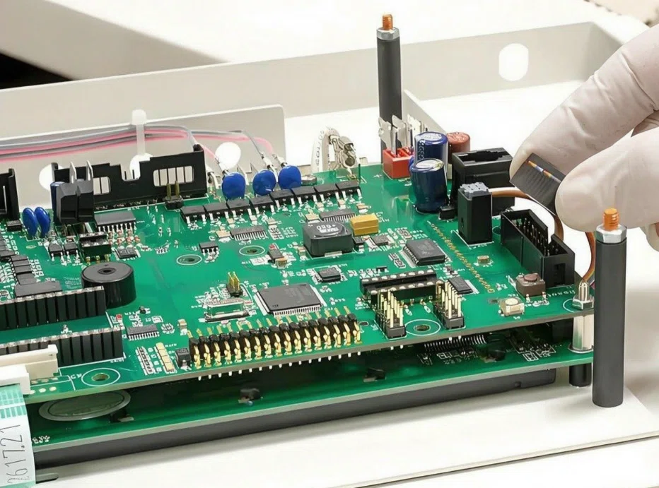
Bare-board physical skeleton: polymer materials and metal micro-topology
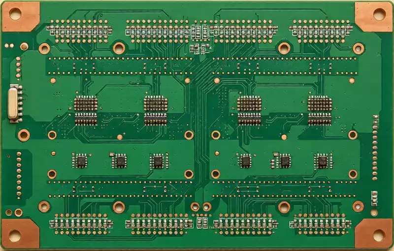
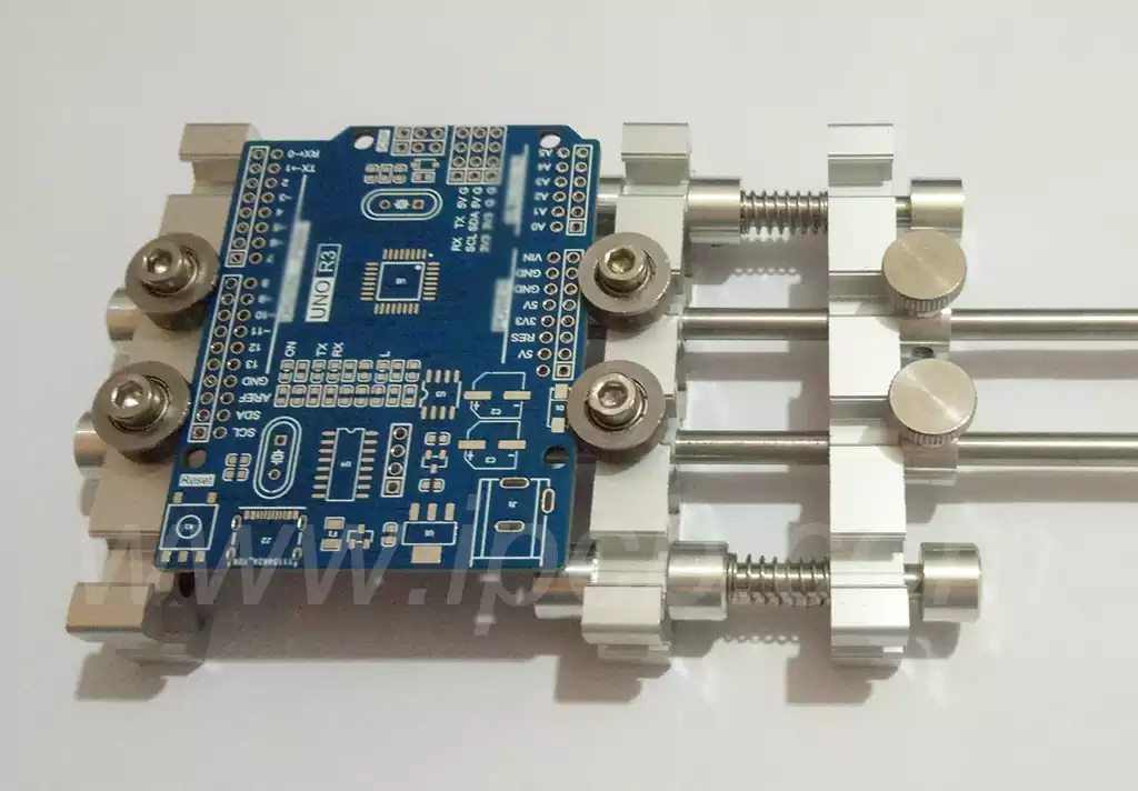
Before any electronic components are soldered on, the circuit board itself is called a “bare board.” A bare board is not simply a piece of plastic, but a multi-layered, composite electromagnetic and physical support system. Insulating Substrate: The Physical Load-Bearing Wall of the Electronic City
The core underlying structure of a circuit board is the insulating substrate. Its main function is to provide mechanical support and prevent electrical short circuits between copper conductors of different layers.
The most common substrate is called FR-4, a composite material formed by high-pressure impregnation and curing of epoxy resin and alkali-free glass fiber cloth. The glass fibers interweave into a high-strength mesh structure, giving the circuit board excellent bending and impact resistance; while the epoxy resin fills the gaps between the fibers, providing extremely high insulation impedance and heat resistance. For high-frequency radio frequency or extreme heat scenarios, engineers also use hydrocarbon ceramic substrates, polytetrafluoroethylene (PTFE) materials, or even metal substrates with aluminum or copper cores to achieve faster heat dissipation or lower electromagnetic signal loss.
Conductive Copper Foil and Traces: The Micro-Vascles of Energy and Signal
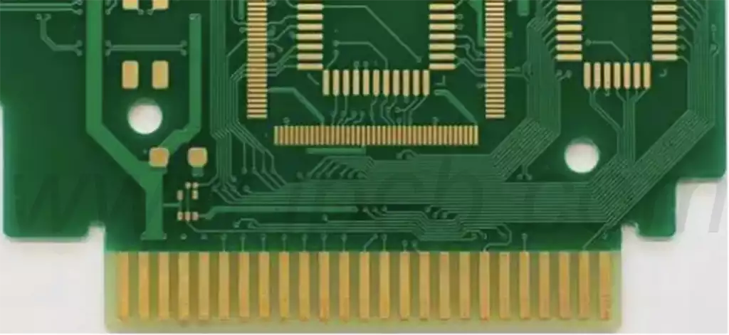
Covering the surface of the insulating substrate and sandwiched within the multilayer board is an extremely thin electrolytic copper foil. After undergoing a high-precision chemical etching process, the originally continuous copper surface is etched into millions of metal wires, each only tens of micrometers or even thinner, known as “traces.”
Traces function as electrical wires on circuit boards. Wider traces are typically used to transmit high-current power, while extremely fine parallel traces are used to transmit high-frequency data signals. The physical topology of the traces requires meticulous calculation; any sharp 90-degree bend can cause high-frequency signals to reflect at the bend, thus compromising data integrity.
Via Systems: Electromagnetic Tunnels in Multidimensional Space Modern circuit boards are often not single-layer or double-layer structures, but rather multi-layered three-dimensional structures composed of four, eight, or even dozens of layers of conductive copper foil alternately stacked with insulating dielectrics. To allow chips on the top layer to communicate with power planes sandwiched in the middle layers or signal lines on the bottom layers, engineers introduced “via” technology.
Via are tiny holes drilled into the board using mechanical drilling or laser ablation, followed by a thin layer of metallic copper plating onto the inner wall of the hole using a chemical copper plating process. In this way, the holes perpendicular to the board become electromagnetic tunnels connecting different conductive layers. Vias, based on their physical structure, can be divided into through-holes that penetrate the entire board, blind vias that connect only the surface layer and internal layers, and buried vias that are completely hidden between internal layers.
Solder Mask and Silkscreen Layer: Skin and Navigation Markers
Above the processed copper foil traces, a layer of polymer colloid is applied; this is the “solder mask.” Most circuit boards appear green because early solder mask inks widely used green pigments. The solder mask acts like a protective skin, preventing the copper foil from oxidizing and corroding in the air, and preventing the endless spread of molten solder during subsequent soldering, which could cause short circuits.
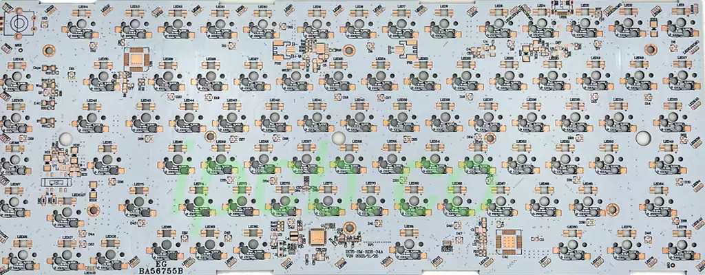
On top of the solder mask, a layer of high-contrast ink (usually white) is printed using industrial inkjet or screen printing technology; this is the “silkscreen layer.” The silkscreen layer prints letters, numbers, borders, and various warning symbols, such as the number of each resistor position, the orientation of the first pin of a chip, and functional descriptions of interfaces. The silkscreen layer does not participate in any electrical connections, but it is an indispensable microscopic navigation map for electronic engineers during assembly, debugging, and repair.
Passive Components: Controllers of Current and Energy Buffers
After the bare board is manufactured, automated placement machines precisely place various electronic components onto pre-defined metal pads. Among all components, the most numerous and seemingly insignificant are called “passive components,” or passive devices.
Passive components do not require an external power source to drive them; they cannot amplify electrical signals or perform active logic judgments, but they determine how current flows smoothly in the circuit.
Resistors: Dampers of the Microscopic World
Resistors are among the most frequently used components on circuit boards. Their basic function is to impede the flow of current and dissipate excess electrical energy as heat.
If current is likened to water flow, a resistor is like a narrow damping valve in a water pipe. By precisely selecting the resistance value, engineers can control the current in various branches of the circuit or, in conjunction with other components, set specific voltage nodes. In digital circuits, resistors are also frequently used as pull-up or pull-down resistors on signal lines to ensure that the line remains stably at a high or low level when there is no signal input, preventing stray noise from being introduced by floating levels.
Capacitors: Miniature Reservoirs and Filters in Electronic Systems
Physically, a capacitor consists of two conductive plates that are close to each other but not in contact, with an insulating dielectric layer between them. It can temporarily store charge in the form of an electric field and release it quickly when needed.
On a circuit board, capacitors primarily perform two core functions: decoupling and filtering. When a high-power chip draws current explosively for a very short time, the power supply line may experience a momentary voltage drop due to physical impedance. A decoupling capacitor placed close to the chip’s power pin can release its stored charge within nanoseconds, filling this voltage dip and ensuring stable chip operation. On the other hand, due to the physical characteristic of capacitors to “pass AC and block DC,” they can easily filter out high-frequency ripple noise mixed in with DC power supplies, or isolate DC bias voltage in audio transmission lines, allowing only AC audio signals to pass.
Inductors: Stabilizers and Electromagnetic Barriers for Magnetic Field Energy
In contrast to capacitors, inductors typically consist of a metal coil wound around a magnetic core. When current flows through the coil, a magnetic field is generated around it; when the current changes, the changing magnetic field generates an induced electromotive force that opposes the change in current. Therefore, inductors have the physical characteristic of “impeding AC and passing DC.”
In the power management module of a circuit board, the inductor is the core of the switching power supply circuit. It alternately charges and discharges with capacitors, efficiently converting high-voltage DC to low-voltage DC. Furthermore, inductors are often used to construct low-pass filters, or combined with capacitors to form resonant circuits at specific frequencies for radio frequency signal selection in wireless communication devices.
Active Components: The Heart of Semiconductors and the Center of Logic Decisions
Unlike passive components, “active components,” or active devices, require an external power supply to exhibit their characteristics. They are the true “intelligent units” on the circuit board, possessing the capabilities for signal amplification, energy conversion, data processing, and logical decision-making. These components are almost entirely built upon semiconductor physical materials (primarily silicon, gallium arsenide, gallium nitride, etc.).
Diodes: Unidirectional Electromagnetic Gates
A diode is a component formed by tightly bonding a P-type semiconductor and an N-type semiconductor to form a PN junction. The PN junction gives the diode extremely strong unidirectional conductivity: current can only flow from the anode to the cathode, while reverse current is completely blocked.
This characteristic makes diodes an ideal barrier to protect circuit boards from damage caused by reverse power connection errors. When a user accidentally reverses the positive and negative terminals of a battery, the diode immediately cuts off the current, protecting subsequent expensive and sensitive chips. In switching power supplies, fast recovery diodes or Schottky diodes serve as freewheeling diodes.
Light Emitting Diodes (LEDs) are the star members of the diode family. When a forward current passes through a PN junction made of a specific semiconductor material, electron-hole recombination releases energy in the form of photons. Various miniature LEDs on circuit boards are used not only to indicate power status and network data transmission status to users, but are also widely used in screen backlight systems.
Transistors: Electronic Switches and Signal Amplifiers
If the PN junction is the building block of the semiconductor industry, then the transistor is the cornerstone of the entire electronics industry. Whether it’s the early bipolar junction transistor (BJT) or the metal-oxide-semiconductor field-effect transistor (MOSFET) that dominates modern integrated circuits, their essence is to control the on/off state or flow of a large current path through a tiny control terminal signal.
In analog circuits, transistors can amplify weak sensor signals or microwave signals received by antennas into strong signals hundreds or thousands of times stronger. In digital circuits, transistors are used as high-speed electronic switches without mechanical wear. When a control voltage is applied, the circuit conducts, representing a digital logic “1”; when the control voltage is removed, the circuit disconnects, representing a digital logic “0”. Modern computers can perform massive calculations precisely because billions of transistors perform billions of extremely rapid on/off switching operations per second. Integrated Circuits: Condensing Vast Cities into a Tiny Space
Integrated circuits (ICs), commonly known as “chips,” are highly integrated components that incorporate thousands, even billions, of transistors, diodes, resistors, and capacitors. These components are fabricated using micro- and nano-fabrication techniques onto a tiny single-crystal silicon wafer and enclosed in a plastic, ceramic, or metal casing.
Chips are the most prominent features on circuit boards. Based on their function, they can be categorized into several main types:
Microprocessors and microcontrollers are the control centers of circuit boards. Microprocessors possess extremely high processing speeds and are designed to execute complex operating systems and heavy computing tasks. Microcontrollers, on the other hand, integrate the processing core, memory, and various input/output interfaces into a single chip, enabling highly efficient control of specific hardware devices, such as the control board of a washing machine or the electronic control unit of a car engine.
Analog chips and power management chips focus on processing continuous signals from the real world. Sound, temperature, and pressure in the real world are continuously changing analog signals. Operational amplifiers in analog chips can precisely process these signals, while analog-to-digital converters can convert these analog quantities into binary digital signals that computers can understand. Power management chips act like the power dispatch center on the circuit board, precisely converting the single input power supply into the various minute voltages required by different chips, and monitoring current levels in real time to prevent overload and burnout.
Memory and storage chips serve as the circuit board’s temporary and permanent memory. Dynamic Random Access Memory (DRAM) provides extremely high-speed data read/write channels for temporarily storing data being processed by the CPU; while flash memory chips can permanently save data using floating gate or charge capture technology even when completely powered off, storing device firmware and user files.
Electrical Interfaces and Electromechanical Components: Bridges Connecting to the Real World
A circuit board that cannot exchange energy and information with the outside world, no matter how powerful its internal chips are, is merely an isolated island. Electrical interfaces and electromechanical components are the bridges connecting the microscopic electronic world inside the circuit board to the external physical world.
Connectors and Plugs: Physical Energy and Data Pathways
Connectors are among the most mechanically complex components on a circuit board. They need to undergo thousands of insertion and removal processes, thus requiring not only good electrical conductivity but also extremely high mechanical strength metal contacts and wear-resistant housings. Power interfaces (such as DC threaded sockets and USB Type-C interfaces) are responsible for introducing power from the external power grid or battery pack into the circuit board. Data interfaces (such as HDMI, Ethernet RJ45 connectors, and PCIe slots) employ high-precision shielding designs for transmitting digital streams at speeds of up to tens of gigabits per second between the circuit board and external displays, network devices, or expansion cards. The circuit board also contains board-to-board connectors or ribbon cable sockets for connecting sub-modules such as cameras, screens, and button panels.
Switches and Electromechanical Controllers: Communicators of Human Intent
To enable human-machine interaction, circuit boards are typically equipped with mechanical switches and micro-buttons. Common tactile switches utilize the elastic deformation of tiny internal metal arches to briefly connect the circuit when pressed, generating a falling-edge electrical signal that triggers a chip interrupt program to achieve power-on, reset, or function switching.
Relays are also found on industrial and high-voltage circuit boards. A relay is a switch that uses an electromagnet to control the opening and closing of mechanical contacts. By energizing the low-voltage coil of a relay, the generated magnetic field attracts the high-voltage contacts to close, thus achieving the isolated control function of safely controlling hundreds of volts of AC high-voltage equipment with a low voltage of 5 volts.
Clock Source: The Crystal Oscillator that Controls the Overall Pulse All logic gates in a digital circuit must work in unison; this unison is called the “clock signal.” The core component on the circuit board that generates this extremely precise clock signal is the “crystal oscillator.”
The crystal oscillator utilizes the inverse piezoelectric effect of quartz crystals: when an alternating voltage is applied across the quartz crystal, the crystal undergoes mechanical deformation; conversely, when the crystal is subjected to mechanical deformation, an electric field is generated on its surface. Because the physical dimensions of quartz crystals can be controlled with extreme precision, its inherent mechanical resonant frequency is extremely stable. The crystal oscillator can output a high-frequency square wave signal with a frequency error of only a few parts per million over an extremely wide temperature range, becoming the “heart rate” followed by all digital chips on the entire circuit board.
Protection and Thermal Management Components: The Guardians of the System
Electromagnetic interference, electrostatic discharge, overcurrent short circuits, and high temperature buildup are the four major killers threatening the lifespan and stability of circuit boards. To ensure long-term reliable operation of circuit boards, engineers must incorporate specialized protection and thermal management components.
Overcurrent and Overvoltage Protection Components: Microscopic Fuses and Floodgates
When an external power surge occurs, or a short circuit occurs inside the circuit board, the instantaneous surge in current can burn out expensive chips within milliseconds.
Fuses are the first line of defense against overcurrent. Traditional thin-film fuses melt due to self-heating when the current exceeds the rated value, completely cutting off the physical path; while polymer self-resetting fuses (PTC) are more intelligent. When an overcurrent occurs, the temperature of the internal polymer material rises, causing the resistance to increase exponentially, limiting the current to a very low level. After the fault is cleared and the temperature cools down, the resistance automatically returns to normal, requiring no manual replacement.
To address transient high-voltage surges caused by electrostatic discharge (ESD) or lightning strikes, circuit boards utilize transient voltage suppressor diodes (TVS) and varistors (MOVs). These components operate in a high-impedance open state under normal operating voltages; however, if a sudden voltage spike of hundreds or even thousands of volts occurs on the line, they rapidly transition to an extremely low-impedance state within nanoseconds, directly discharging the massive surge current to ground and clamping the voltage within a safe range.
Thermal Management Structure: Heatsinks, Thermal Pads, and Metal Ventilation Holes A significant portion of the electrical energy consumed by electronic components during operation is converted into heat and dissipated. If heat accumulates inside the chip and cannot dissipate, the performance of the semiconductor material will rapidly deteriorate, potentially leading to thermal collapse and permanent damage.
For high-power chips (such as CPUs, graphics processors, or power MOSFETs), their surfaces are typically covered with heatsinks made of aluminum alloy or pure copper. These heatsinks have dense metal fins that greatly expand the surface area in contact with air. Between the chip and the heatsink, thermal grease or a soft thermal pad is filled to squeeze out air gaps between their microscopic surfaces, reducing bottom contact thermal resistance.
In the design of the circuit board itself, engineers also densely arrange “thermal vias” under high-power chips. These vias act as vertical heat conduction channels, quickly transferring heat dissipated by the chip to a larger copper foil plane on the bottom of the circuit board, utilizing the entire circuit board for passive heat dissipation.
Physical Packaging Forms: From Through-Hole to Micro Surface Mount
Understanding the composition of a circuit board requires not only understanding the function of each component but also how these components are physically fixed to the circuit board and established electrical connections. The evolution of electronic packaging technology directly determines the changes in the size of circuit boards.
Traditional Through-Hole Technology: A Symbol of Mechanical Strength and High Power
Before the 1980s, the vast majority of circuit boards used through-hole technology. This technology required drilling a large number of pin holes during the manufacturing process. Through-hole (SMD) components have long, thick metal leads. During installation, these leads are passed through through-holes on the board, and then soldered onto the back of the circuit board using wave soldering.
The advantage of SMD components lies in their extremely high mechanical anchoring strength, capable of withstanding enormous insertion and removal forces and physical vibrations. Therefore, SMD technology still holds a place in power interfaces, large-capacity electrolytic capacitors, large transformers, and heavy-duty automotive electronics. However, SMD technology requires drilling numerous holes in the board, which significantly reduces the routing space within multilayer boards, limiting further reductions in board size.
Modern Surface Mount Technology: Extreme Density and Automated Production
To adapt to the trend of thinner and lighter electronic products, surface mount technology (SMD) emerged and quickly became the mainstream of modern circuit board manufacturing.
Surface mount components (SMD) completely eliminate long metal leads, replacing them with flat metal terminals on the side or bottom of the component body. The circuit board surface no longer requires penetrating holes; only flat conductive pads are needed. On the production line, pick-and-place machines precisely place micro-components onto solder paste-coated pads at an astonishing speed of tens of thousands of points per hour, then send them to a reflow oven. The reflow oven, through precise temperature control, melts the tin powder in the solder paste, automatically bonding the component leads to the pads under surface tension.
Surface mount technology significantly shortens component lead length, thereby drastically reducing parasitic inductance and capacitance introduced by the leads and significantly improving the performance of high-frequency circuits. Simultaneously, because it does not require penetrating the board, both sides of the circuit board can be densely packed with components, increasing the integration density of the circuit board several times over.
High-Density Ball Grid Array and the Limits of Miniaturization
In the field of very large-scale integrated circuits (VLSI), traditional peripheral chip packaging can no longer meet the needs of hundreds or even thousands of input/output pins. If thousands of pins were arranged around the chip, the pin pitch would be reduced to an unmanufacturable level.
To address this, engineers invented Ball Grid Array (BGA) packaging. BGA chips arrange all pins in a matrix grid across the entire bottom surface of the chip, with each pin being a tiny solder ball. During soldering, the chip lies directly on the corresponding pad array on the circuit board, and hundreds of connections are completed in one go through reflow soldering.
To further push the limits of size, modern smartphone motherboards widely employ High-Density Interconnect (HDI) technology. HDI boards utilize micro-vias (with apertures less than 100 micrometers) drilled by ultra-fine lasers, combined with multilayer manufacturing processes, to reduce trace width and spacing to an extreme degree. On such circuit boards, thousands of passive components have been shrunk to a size that is difficult to distinguish with the naked eye, condensing the vast functionality of an entire computer system into a physical space the size of a card.
Summary: Microscopic Cooperative Electromagnetic Systems
When we re-examine a printed circuit board, it is no longer just a green board inlaid with various plastic and metal blocks, but a microscopic industrial behemoth that has undergone highly precise logical planning, physical reconstruction, and electromagnetic tuning.
In this city:
Insulating substrates and multi-layered copper foil form the foundation, the multi-level overpasses, and the underground tunnel network; passive components silently maintain the stability of water pressure and flow, filtering out all electromagnetic noise; active components and integrated circuits, like the brain and nerve center of a skyscraper, perform high-speed calculations and decisions; connectors and protective devices extend their arms, connecting to the complex real world on one hand, and resisting electromagnetic storms from the outside world on the other. Every component, every trace, and even the shape and position of every via on the circuit board is not randomly generated, but rather the ultimate expression of the laws of materials science, semiconductor physics, and electromagnetics at the centimeter scale. It is precisely this seamless collaboration among countless microscopic elements that collectively supports the magnificent edifice of the entire modern information society.