In the long history of modern electronics development, if single-sided printed circuit boards (PCBs) opened the door for electronic products to break free from the constraints of disordered wiring, then double sided copper clad PCB boards (DCPs) are the true cornerstone that has brought humanity into a world of complex computing, efficient communication, and high-density electronic integration. From early simple radio control circuits to automotive electronic control units, and then to the control cores of various industrial automation equipment, DCPs, with their unique double-layer conductive topology, cross-layer electrical interconnection capabilities, and extremely high overall cost-effectiveness, constitute the skeleton and neural network of the entire modern hardware world.
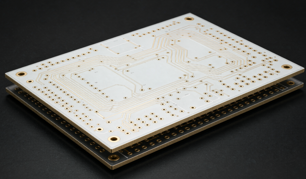
However, a seemingly thin DCP is far more than a simple mechanical stacking of two single-sided boards. It is the culmination of a highly interwoven multidisciplinary field, including materials science, polymer chemistry, precision mechanical drilling, electrochemical deposition, photolithography, and thermodynamic control. A deep analysis of the microscopic physical properties and manufacturing processes of DCPs not only allows us to understand the rigorous logic of electronic hardware manufacturing but also provides a glimpse into humanity’s engineering wisdom in taming electromagnetic energy at the micrometer scale.
Microscopic Anatomy and Materials Science Genes of Double Sided Copper Clad Laminates
To understand the engineering value of double sided copper clad laminates PCB boards, we must first discuss their physical nature and material composition. As the name suggests, the core characteristic of CCLs lies in the fact that a layer of high-purity copper foil is firmly bonded to both sides of the insulating substrate.
Physical and Chemical Framework of the Insulating Substrate
The foundation of CCLs is an insulating dielectric layer with precisely controllable thickness. The most widely used material is FR-4 epoxy resin fiberglass cloth laminate. Within this material, several layers of extremely fine alkali-free glass fiber yarns interweave to form a rock-solid inorganic framework, giving the circuit board excellent mechanical bending and tensile strength, as well as extremely high dimensional stability.
Between this glass fiber mesh is filled with epoxy resin that has undergone high-temperature and high-pressure deep curing. The epoxy resin not only tightly bonds the glass fibers together but also provides excellent electrical insulation properties, ensuring that current is never allowed to directly penetrate the dielectric layer under operating voltage. For applications requiring specific heat dissipation or high-frequency characteristics, engineers may also choose polyimide, hydrocarbon ceramic substrates, or even aluminum-based double-sided copper-clad laminates (CCLs) to meet the demands for heat conduction or low dielectric loss in extreme environments.
Metallurgical Properties of Double-Sided Copper Foil: Lay extremely thin electrolytic or rolled copper foil on both sides of the insulating substrate. When CCLs are manufactured, the thickness of these copper foils is typically measured in ounces (for example, a common one-ounce copper foil is approximately 35 micrometers thick).
This copper foil is not simply a metallic covering; its inner side (the side in contact with the resin substrate) undergoes a specialized micro-roughening treatment. Under a microscope, the inner surface of the copper foil is covered with countless micrometer-sized “copper teeth.” When the resin is pressed under high temperature and pressure, it seeps into the gaps between these copper teeth like a fluid, forming a strong mechanical anchoring force. This microstructure ensures that the copper foil will never peel off from the substrate surface even after dozens of chemical etchings and reflow soldering at hundreds of degrees Celsius.
A Leap in Spatial Dimension: From Single-Sided Planar Topology to Double-Sided 3D Interconnection
The biggest limitation of single-sided printed circuit boards (PCBs) is that their circuit topology is confined to a single two-dimensional plane. As the number of components surges and circuit logic becomes extremely complex, single-sided wiring inevitably results in numerous trace intersections. To avoid short circuits, engineers have to rely on a large number of external jumpers, which severely restricts the miniaturization and automated production efficiency of electronic products.
The emergence of double-sided copper-clad laminates (CCLs) has completely broken this physical constraint of two-dimensional space.
Dual-Track Parallel Routing on Top and Bottom Layers
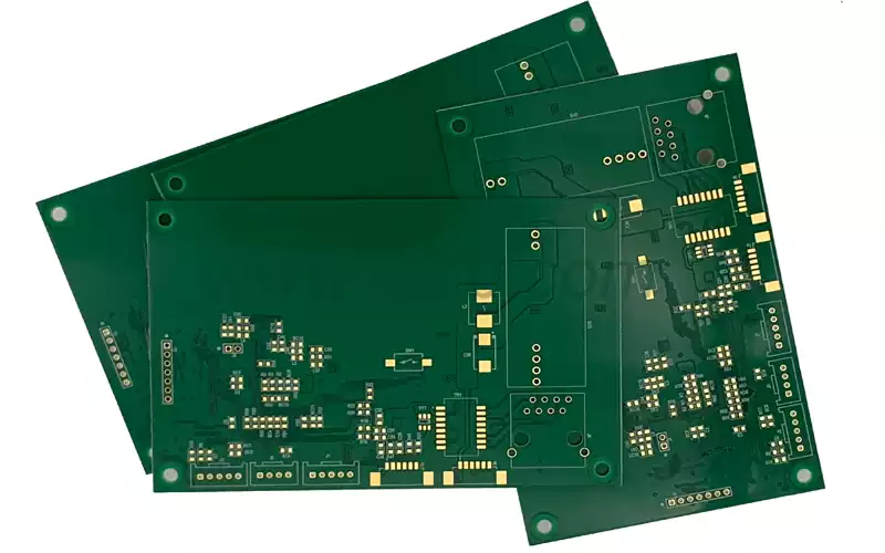
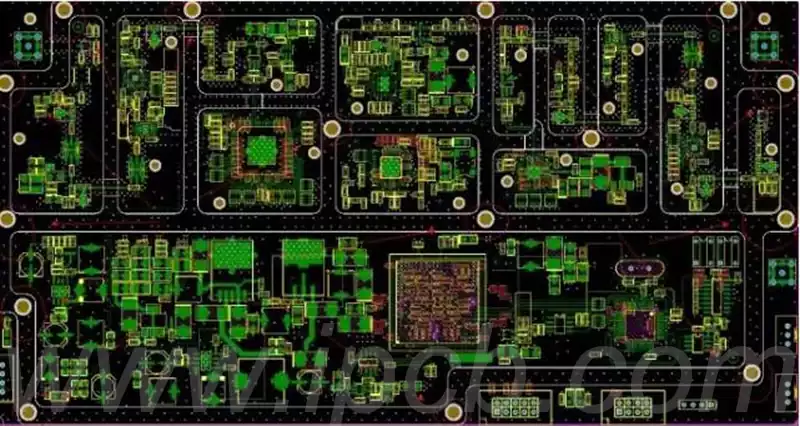
On double-sided PCBs, engineers can utilize both surfaces simultaneously for copper foil routing. Signal conflicts that were previously unavoidable on single-sided boards can be perfectly resolved by routing some traces on the top layer and others on the bottom layer. This dual-track parallel routing method instantly more than doubles the wiring density of the PCB.
More importantly, double-sided CCLs allow designers to construct more optimized electromagnetic return paths. For example, dense signal lines can be laid on the top layer, while a large area of continuous grounding copper can be laid on the bottom layer. This topology, where the signal line is flush with the reference ground plane, provides an extremely low-impedance return path for weak high-frequency signals, significantly suppressing electromagnetic interference and greatly improving the signal integrity of the entire system.
Via: An electromagnetic tunnel connecting two planes
However, simply having a top and bottom layer does not automatically ensure a smooth circuit. If a node in the circuit needs to connect to both a chip pin on the top layer and a power network on the bottom layer, independent traces on the two planes still cannot intersect.
To solve this spatial crossing problem, double-sided copper-clad laminates introduce a core microscopic component—the through-hole via. A via acts like an electromagnetic tunnel vertically penetrating the entire insulating substrate, electrically and tightly stitching together the previously isolated top and bottom copper traces. The circuit board’s three-dimensional topology thus truly leaps from purely planar geometry to a three-dimensional network.
Electromagnetic Tunnels Across Layers: Mechanical Drilling and Plated Through-Hole (PTH) Processes
To ensure that vias on double-sided copper-clad laminates (CCLs) truly function as conductors, the manufacturing process must overcome a crucial and extremely challenging hurdle—Plated Through-Hole (PTH). Over 90% of the electrical reliability of a CCL depends on the quality of its PTH.
High-Precision CNC Mechanical Drilling
The first step in manufacturing is to precisely drill thousands of tiny holes across the entire CCL. Since the hole diameter is often only 0.2 to a few tenths of a millimeter, factories must use high-speed CNC drilling machines with micro tungsten carbide drill bits to perform mechanical drilling at ultra-high speeds of tens of thousands or even hundreds of thousands of revolutions per minute.
During the drilling process, the high-speed friction between the drill bit and the epoxy resin and glass fiber generates enormous localized high temperatures. If chip removal is inadequate or the rotation speed is out of control, the high temperature will instantly melt the resin and adhere it to the copper foil cross-section of the hole wall, forming an insulating layer of “smear.” If this layer of adhesive residue is not completely removed, subsequent via electroplating will result in a catastrophic circuit break.
Throughhole Electroless Copper Plating and Conductive Seed Layer Construction
After drilling, the exposed cross-section inside the circuit board consists of ring-shaped fractures made of insulating substrate and glass fiber, completely lacking conductivity. To electroplat a thick layer of metallic copper inside these insulating via walls, a “chemical copper plating” process must first be completed.
The circuit board is immersed in a complex chemical plating solution containing a palladium catalyst and copper salt. The palladium catalyst adsorbs onto the insulating via walls, triggering an autocatalytic chemical reduction reaction. Copper ions in the solution are reduced to free metallic copper, which is uniformly deposited on the surface of the entire via wall, the top copper foil, and the bottom copper foil.
After chemical copper plating, the entire surface of the double-sided copper-clad laminate, including the inside of the via walls, is coated with an extremely thin but continuous conductive “seed layer.” Although this seed layer is less than one micrometer thick, it has successfully electrically connected the top layer, bottom layer, and all hole walls, paving the way for subsequent thicker electroplating.
Full-board Copper Plating and Hole Copper Thickness Guarantee: Chemical copper plating is merely the rudimentary form of the electromagnetic tunnel; its thickness is extremely thin and cannot withstand high currents or mechanical stress. Next, the circuit board enters the electroplating workshop for “pattern electroplating” or “full-board copper plating.”
In the electroplating tank, the circuit board is connected to the cathode and immersed in a copper sulfate electrolyte. Driven by a DC electric field, copper ions in the electrolyte continuously move towards the surface of the circuit board and accelerate deposition on the seed layer. With precise control of the electroplating time, the metallic copper layer inside the hole walls gradually thickens until it reaches the engineering standard of approximately twenty to twenty-five micrometers. This robust “hole copper” layer constitutes the steel corridor that transmits energy and signals across layers in the double-sided copper-clad laminate.
Photolithography and Double-Sided Pattern Transfer: Micron-Level Precise Alignment
After the double-sided copper-clad laminate (CCL) has completed drilling and metallization, achieving full electrical connectivity, the next step is to etch intricate circuit traces onto the copper surfaces of the top and bottom layers. This process is known as double-sided pattern transfer and chemical etching.
Photosensitive Dry Film Lamination and Simultaneous Double-Sided Exposure
First, the workshop thoroughly cleans the circuit board and uniformly laminates a layer of ultraviolet-sensitive dry film (Photoresist) onto the copper foil surfaces of both the top and bottom layers.
The core challenge of double-sided pattern transfer lies in “optical alignment.” The trace patterns on the top and bottom layers must achieve absolute precision alignment at the micron level, especially for through-hole pads that penetrate both layers. Even a misalignment of tens of microns between the top and bottom patterns will cause the drill center to deviate from the pad, resulting in etching defects or poor soldering.
The exposure machine uses high-precision optical positioning pins to tightly adhere the film (phototool) bearing the circuit pattern to both sides of the circuit board. Then, strong ultraviolet light is used for simultaneous double-sided exposure. The ultraviolet light penetrates the transparent areas of the film, causing the dry film to polymerize and harden; while the black areas block the light, keeping the dry film uncured.
Developing and Chemical Etching: After rinsing with the developing solution, the soft dry film in the unexposed areas is completely dissolved and washed away, exposing the unwanted copper substrate; the hardened dry film acts like a strong armor, firmly protecting the underlying circuit traces and pads.
Subsequently, the circuit board is sent to a powerful chemical etching machine. Acidic or alkaline copper chloride etching solution is sprayed under high pressure onto the board surface, relentlessly dissolving and removing the exposed copper foil that has lost its dry film protection. Finally, a stripping solution is used to thoroughly wash away the hardened dry film protecting the traces. At this point, a clear, independent, and tightly connected precision circuit pattern, with the top and bottom layers tightly connected by metallized vias, is officially revealed.
Thermodynamic Equilibrium, Stress Mechanics, and High-Frequency Signal Integrity
Designing and manufacturing a high-quality double sided copper clad laminate (CCL) requires much more than just “conductivity.” In the real physical world, thermodynamic stress, mechanical deformation, and electromagnetic signal integrity pose far more stringent challenges to CCLs.
Z-Axis Thermal Expansion and Via Wall Fracture Protection
During subsequent component soldering (such as reflow soldering or wave soldering), the circuit board is subjected to instantaneous high-temperature shocks reaching up to 260 degrees Celsius. At this time, the coefficient of thermal expansion of the epoxy resin substrate in the direction perpendicular to the board surface (i.e., the Z-axis direction) is much greater than that of metallic copper.
This huge difference in thermal expansion generates enormous vertical tensile stress inside the vias. If the elongation of the plated copper in the via is insufficient, or the copper layer thickness on the via wall is uneven, the high temperature will pull the copper layer in the middle of the via wall directly off like noodles, causing a permanent open circuit in an unseen location. To prevent this disaster, the manufacturing of high-quality CCLs must strictly control the electroplating additives to ensure that the copper crystal structure in the vias has extremely high toughness and fatigue strength.
Reflow Soldering Thermal Stress and Board Warpage Control
Besides Z-axis expansion, uneven copper foil distribution on both sides of a double-sided copper-clad board (CCP) (e.g., one side has a large area of solid ground copper foil, and the other side has sparse, fine signal traces) can cause significant warpage and twisting when the board is heated. A warped board cannot be smoothly transported on automated SMT placement lines, leading to component misalignment or even poor soldering. Therefore, the “copper foil symmetry balance principle” is an inviolable rule in the design and manufacturing of double-sided circuit boards. In blank areas without signal traces, engineers must manually lay a grid of balancing copper foil to maintain absolute symmetry in the board’s thermal mass and thermal expansion.
Signal Integrity and Reflow Path Planning
In high-speed digital or RF circuits, the traces on a CCP are not just conductors, but miniature transmission lines. Each surface signal line needs a continuous, uninterrupted reference ground plane directly beneath it (or through the underlying ground plane).
If the underlying ground plane is arbitrarily cut off by too many vias, the return current of high-frequency signals is forced to take a long detour, thus forming a huge electromagnetic radiation loop on the circuit board. This not only emits electromagnetic interference (EMI) but also causes severe signal distortion or overshoot. Therefore, excellent double-sided circuit board design must carefully plan the integrity of the ground plane to ensure that every high-speed signal has an easily accessible low-impedance return path.
Design for Manufacturing (DFM) and Automated Quality Inspection
After the double-sided copper-clad board has completed solder resist coating, surface treatment (such as tin plating and immersion gold), and silkscreen printing, it must undergo rigorous testing according to Automated Industrial Manufacturing Standards (DFM) before being officially delivered for use.
Automated Optical Inspection (AOI) Due to the increasing trace density of double-sided circuit boards, manual visual inspection is no longer sufficient for screening micron-level defects. Automated Optical Inspection (AOI) equipment utilizes high-resolution industrial cameras and multi-angle optical scanning to compare the surface image of each finished double-sided circuit board pixel-by-pixel with the original computer-aided manufacturing (CAM) data. Any minute micron-level short circuit, open circuit, scratch, micro-pinhole, or solder mask misalignment cannot escape the keen eyes of the AOI system and is precisely marked and rejected.
Flying Probe Testing and Electrical Verification
In addition to the optical inspection of the appearance, physical verification of electrical performance is equally indispensable. For double-sided circuit board prototypes or small-to-medium batch production, flying probe testers are essential tools.
Several extremely flexible, servo-motor-driven ultra-fine test probes move at extremely high speeds across both sides of the circuit board, precisely contacting each pad and test point. By instantaneously applying minute test currents and voltages, the flying probe tester can verify 100% whether each via is fully conductive and whether there are any parasitic short circuits between each net. Only double-sided copper-clad laminates that successfully pass AOI optical inspection and flying probe electrical verification are qualified to be labeled as qualified and go to electronic assembly workshops around the world.
Conclusion: Timeless Classics and Engineering Aesthetics
In today’s world of multilayer boards, high-density interconnects (HDI), and 3D packaging technologies, double-sided copper-clad PCBs remain the mainstay of the printed circuit board industry, boasting the largest shipment volume and widest application.
With its exquisitely crafted physical double-layer structure, it perfectly balances performance, complexity, and manufacturing cost. From the selection of polymer substrates to the electrochemical deposition of micron-level metallized vias, from the precise alignment of double-sided photolithography to the precise control of thermodynamic stress, the manufacturing process of double-sided copper-clad PCBs vividly illustrates the unparalleled engineering wisdom of humankind in transforming abstract circuit principles into highly reliable physical entities. Understanding the underlying logic of double-sided copper-clad PCBs is not only about mastering an electronic manufacturing technology, but also an essential path to appreciating the rigor, precision, and superior aesthetics of modern industrial civilization.