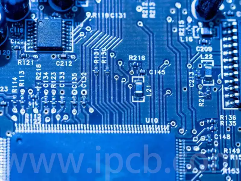
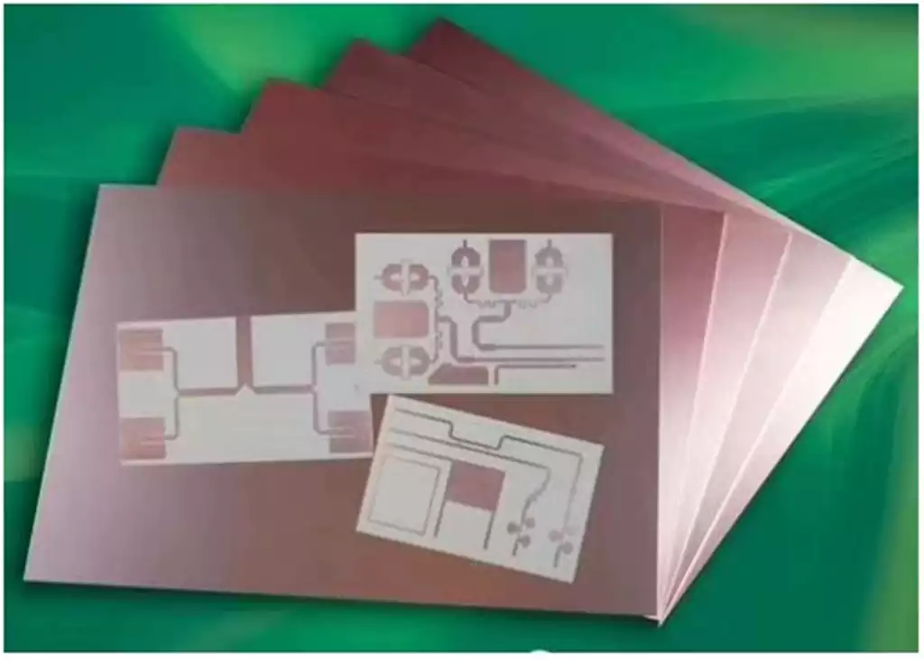
Ceramic pcb, also known as ceramic printed circuit board, is circuit board manufactured using ceramic materials. Compared to conventional fibreglass-reinforced plastic (FR-4) substrates, ceramic PCBs utilise ceramic substrates, offering significant performance advantages. These include superior temperature stability, enhanced mechanical strength, improved dielectric properties, and extended service life. They are primarily employed in high-temperature, high-frequency, and high-power circuit applications. Their critical role is evident in sectors such as LED lighting, power amplifiers, semiconductor lasers, radio frequency transceivers, sensors, and microwave components.
Application Domains by Material Classification
Aluminium Oxide Ceramics (Al₂O₃): Aluminium oxide ceramics exhibit outstanding insulation properties and high-temperature stability, coupled with high hardness and mechanical strength. These characteristics make them an ideal choice for high-power electronic equipment, meeting the stringent material performance requirements of such devices.
Aluminium Nitride Ceramics (AlN): Aluminium nitride ceramics are renowned for their high thermal conductivity and excellent thermal stability. In high-power electronics and related fields such as LED lighting, it effectively addresses heat dissipation challenges, ensuring stable equipment operation and thus achieving widespread adoption.
Zirconia Ceramics (ZrO₂): Zirconia ceramics exhibit high strength, hardness, and outstanding wear resistance. Within high-voltage electrical equipment, these properties enable them to withstand diverse stresses under high-voltage conditions, guaranteeing equipment safety and reliability.
Application Fields by Process Classification
HTCC (High-Temperature Co-fired Ceramics): The HTCC process is suitable for high-temperature, high-power applications, spanning multiple industries including power electronics, aerospace, satellite communications, optical communications, medical equipment, automotive electronics, and petrochemicals. Its diverse product range encompasses high-power LEDs, power amplifiers, inductors, sensors, and energy storage capacitors, providing robust support for the high-performance demands of these sectors.
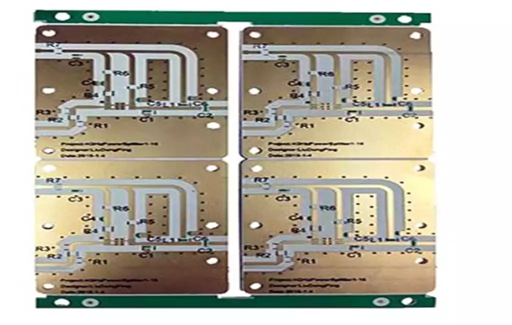
LTCC (Low-Temperature Co-fired Ceramics): The LTCC process excels in manufacturing microwave components such as RF, microwave, antenna, sensor, filter, and power divider devices. Furthermore, it finds extensive application in medical, automotive, aerospace, communications, and electronics sectors. Typical products include microwave modules, antenna modules, pressure sensors, gas sensors, accelerometers, microwave filters, and power dividers, meeting diverse requirements for microwave components across various sectors.
DBC (Direct Bonded Copper): The DBC process is primarily employed for thermal management in high-power semiconductor devices (such as IGBTs, MOSFETs, GaN, SiC, etc.). Leveraging its superior thermal conductivity and mechanical strength, it effectively addresses heat dissipation challenges in power semiconductors. Product examples include power modules, power electronics, and electric vehicle controllers, ensuring stable operation during high-efficiency performance.
DPC (Direct Copper Multilayer Printed Circuit Board): The DPC process is primarily employed for thermal management in high-power LED lighting. Characterised by high strength, thermal conductivity, and electrical performance, it significantly enhances the thermal efficiency and electrical properties of LED lamps. Product examples include LED lamps, UV LEDs, and COB LEDs, driving advancements in LED lighting technology.
LAM (Laminated Ceramic-Metal Board): LAM technology is employed for thermal management and electrical performance optimisation in high-power LED lighting, power modules, and electric vehicles. By combining the advantages of ceramic and metal substrates, it enhances thermal dissipation and electrical characteristics. Product examples include LED lighting, power modules, and electric vehicle motor drivers, providing technical support for these sectors.
Ceramic substrates are favoured in microelectronics due to their exceptional properties, chiefly including high strength, excellent thermal conductivity, superior insulation, and robust thermal cycling performance.
Key Characteristics of Ceramic Substrates
Ceramic substrates possess several notable properties that make them the material of choice for high-end electronic components.
Mechanical Properties and Stability
Ceramic substrates exhibit robust mechanical stress resistance, dimensional stability, and possess high strength with excellent adhesion. Furthermore, they demonstrate corrosion resistance. Silicon nitride ceramic substrates achieve a flexural strength of 852.7±48.8 MPa following optimisation of material composition and sintering processes.
Thermal Properties
The high thermal conductivity of ceramic substrates enables efficient heat dissipation, ensuring stability during high-power operation of electronic devices. For instance, aluminium oxide ceramics exhibit thermal conductivity ranging from 15 to 35 W/m·K, while aluminium nitride ceramics can reach 170 W/m·K. Silicon nitride ceramics combine excellent intrinsic thermal conductivity with superior mechanical properties. Ceramic substrates also exhibit outstanding thermal cycling performance, withstanding up to 50,000 cycles, thereby enhancing reliability. Their thermal expansion coefficient matches that of chips. Furthermore, they can operate across an extensive temperature range of -55°C to 850°C.
Electrical Properties and Manufacturing Characteristics
Ceramic substrates possess excellent electrical insulation, preventing current leakage and short circuits. They exhibit a low dielectric constant. Various patterned structures can be etched into ceramic substrates, similar to printed circuit boards (PCBs). Furthermore, ceramic substrate production is pollution-free and environmentally benign.
Advantages of Ceramic Substrates
Ceramic substrates offer numerous advantages over traditional metal or plastic substrates, establishing them as a critical material in high-power electronic circuit structures.
Superior Thermal Management Capabilities
The high thermal conductivity of ceramic substrates enables compact chip packaging, significantly enhancing power density and improving system and equipment reliability. For instance, the high thermal conductivity of DPC substrates enhances local heat dissipation capabilities. The thermal expansion coefficient of ceramic substrates is close to that of silicon chips, eliminating the need for transition layer Mo sheets, thereby saving labour, materials, and reducing costs. Ceramic substrates also feature low thermal resistance.
Enhanced Reliability and Safety
Ceramic substrates reduce solder layers, lower thermal resistance, and minimise voids, thereby improving yield rates. Furthermore, their high insulation and withstand voltage characteristics ensure personal safety and equipment protection. Ceramic substrates also demonstrate exceptional high-temperature resistance.
High Current-Carrying Capacity and Integration
Ceramic substrates possess substantial current-carrying capabilities. For instance, when a 100A current flows continuously through a 1mm-wide, 0.3mm-thick copper layer, the temperature rise is approximately 17°C; with a 2mm-wide, 0.3mm-thick copper layer, the rise is merely around 5°C. These properties enable novel packaging and assembly methods, enhancing product integration and reducing form factor.
Environmental Advantages
Ultra-thin ceramic substrates of 0.25mm thickness can replace BeO, which poses toxicity concerns, thereby avoiding environmental issues.
Differences Between Ceramic Substrates and Standard PCB Boards
Currently, FR-4 circuit boards are the most widely used in the market. However, defects in FR-4 boards are irreversible once they occur. FR-4 laminates offer advantages such as no need for an insulating layer, suitability for mass production, rapid forming, and low cost. Yet their shortcomings are equally pronounced:
- Thickness Deviation: Commonly observed as thicker centres with thinner peripheries, or uneven thickness across opposite sides. This impacts PCB processing, with thickness inconsistencies affecting slot depth and substrate wear resistance. For precision printed circuit boards, excessive thickness deviation may cause inconsistent connector tightness during assembly, leading to poor contact and compromised electronic device performance. For multilayer PCBs, cumulative thickness deviations may render entire boards unusable. Such boards fail to meet the stringent thickness tolerance requirements for high-voltage applications in test platforms and other precision products.
- Substrate blooming: Compromises solderability, electrical insulation, and numerous other properties, rendering the substrate unfit for genuine use.
- Substrate delamination: While not necessarily prohibitive for application, it disqualifies the substrate from achieving Grade A product status.
- Substrate white spots/streaks: Severely compromises PCB manufacturing quality.
- Substrate exposed weave pattern: Diminishes insulation performance, significantly degrading PCB quality.
- Substrate impurities/black specks: Affects product appearance and may cause other issues.
- Copper foil creases: Panels exhibiting such folds are prohibited for PCB production.
- Resin spots: Cured resin residues that cannot be etched away during production severely compromise inter-wire insulation and are therefore unsuitable for PCB fabrication.
- Pits: Significantly impact PCB quality, potentially causing circuit discontinuity or semi-continuity.
- Pinholes: Result in coarse patterns and kerosene-like leakage marks.
- Copper foil oxidation: Minor oxidation does not affect PCB quality but should be minimised. Severe oxidation may hinder thorough etching during PCB fabrication and renders the material unsuitable for laminate production.
- Copper foil bright spots: These indicate compromised anti-oxidation layers, making the area susceptible to oxidation during storage and adversely affecting PCB performance. Larger bright spots may indicate thinner copper-tin layers at these points, which can also compromise PCB manufacturing quality.
As electronic devices accelerate towards higher power and frequency, ceramic pcb is progressively overcoming the performance limitations of traditional substrates. Leveraging their unique advantages, they are emerging as a key material driving advancements in high-end sectors such as 5G communications and new energy vehicles. Their future market potential and scope for technological innovation are highly promising.