Alumina pcb is characterized by pure white substrates and are the most commonly used ceramic substrate material in the electronics industry because of their high strength and chemical stability in terms of mechanical, thermal and electrical properties compared to most other oxide ceramics, as well as the availability of raw materials from a wide range of sources for various techniques of fabrication and different shapes.
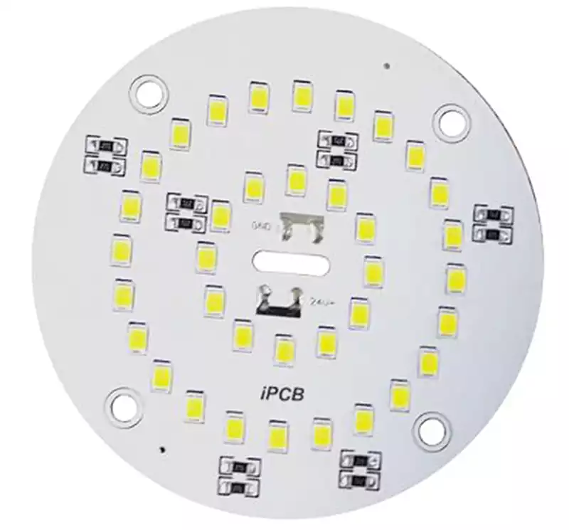
Alumina is one of the most cost-effective and widely used substrate materials for microelectronic applications, according to the type of metallization process can be divided into thick-film substrates and thin-film substrates, of which, thick-film substrates are highly reliable and are widely used in the manufacture of hybrid microelectronic circuits; and in recent years, because it can better meet the requirements of the line size continues to shrink under the requirements of the high degree of accuracy, the ceramic circuit boards prepared using a thin-film process has been in the power type LED In recent years, ceramic circuit boards prepared using the thin-film process have shown strong competitiveness in power LED packaging.
Thin film substrate is a major feature of the circuit of fine lines, high precision, but also because of the “fine line” does not allow ups and downs, thin-film circuits on the substrate surface quality requirements, so the substrate used for thin-film circuits require high purity (commonly 99.6% purity of alumina), low purity of the substrate in the glass phase is more, the surface roughness is large; The higher the purity of the substrate, the more polished, dense, the lower the dielectric loss, but the higher the price.
99.6% alumina ceramic’s high purity and smaller grain size makes the material smoother, less surface defects, and get a very small surface roughness, with high mechanical strength, low thermal conductivity, excellent electrical insulation, good dielectric properties, and good corrosion and abrasion resistance, is the first choice for the manufacture of thin-film circuit substrates.
Alumina ceramic substrate processing technology is currently on the market mostly using thin film technology, thick film technology, DBC technology, HTCC technology and LTCC technology.
Thick film process
Alumina ceramic substrate thin film process thin film method is the main method of metal film deposition in microelectronics manufacturing, and among them, direct copper plating is the most representative.Direct copper plating (DPC) is mainly used for metallization of the substrate surface by vapor deposition, magnetron sputtering and other surface deposition processes, first sputtering titanium, chromium and then copper particles under vacuum conditions, and finally thickening by electroplating, followed by the ordinary pcb process to complete the circuit fabrication, and finally by electroplating/chemical plating to increase the thickness of the circuit.
DBC Process
DBC process is applicable to most ceramic substrates, good metal crystallinity, good flatness, lines are not easy to come off, line position is more accurate, smaller line spacing, stable reliability.Alumina ceramic DBC process Ceramic copper cladding board, DBC for short, consists of ceramic substrate, bonding layer and conductive layer.
It is a special process method of directly bonding copper foil to the surface of alumina or aluminum nitride ceramic substrate at high temperature, which has high thermal conductivity, high adhesive strength, excellent solderability and excellent electrical insulation properties, but it cannot pass through the holes, poor precision and rough surface. As the line width can only be applied to a larger pitch, can not do precision, only mass production can not be realized in small-scale production.
HTCC process
HTCC process is used in the high temperature co-firing process, HTCC ceramic heating pad is a high-temperature co-firing ceramic heating pad, using tungsten, molybdenum and other high melting point metal heating resistor paste design, molybdenum and manganese according to the heating circuit. Requirements are printed on 92-96% alumina cast ceramic raw billet, 4-8% sintering additives laminated, co-fired at a high temperature of 1500-1600°C, with corrosion resistance and high temperature resistance. Temperature resistance. It is characterized by long life, high energy efficiency, uniform temperature, good thermal conductivity, fast thermal compensation, etc. Moreover, it is free of lead, cadmium, mercury, hexavalent chromium, polybrominated biphenyls (PBBs), polybrominated diphenyl ethers (PBDEs), and other hazardous substances.
LTCC process
LTCC process is a low-temperature co-fired ceramics will be low-temperature sintered ceramic powder into a precise and dense raw ceramic tape, and laser drilling, microvia grouting, precision conductor paste printing ceramic tape on the raw. The desired circuit pattern is created and multiple passive components (e.g., low-capacitance capacitors, resistors, filters, impedance converters, couplers, etc.) are embedded in the multilayer ceramic substrate and then stacked together. The inner and outer electrodes can be made of metals such as silver, copper, gold, etc. and sintered at 900°C to make a high-density circuit that does not interfere with each other in three-dimensional space. Three-dimensional circuit substrates with built-in passive components can also be made. ICs and other materials can be mounted on the surface. The source device is made into a passive / active integrated functional modules, can be further miniaturized and increase the circuit density, especially for high-frequency communication components.
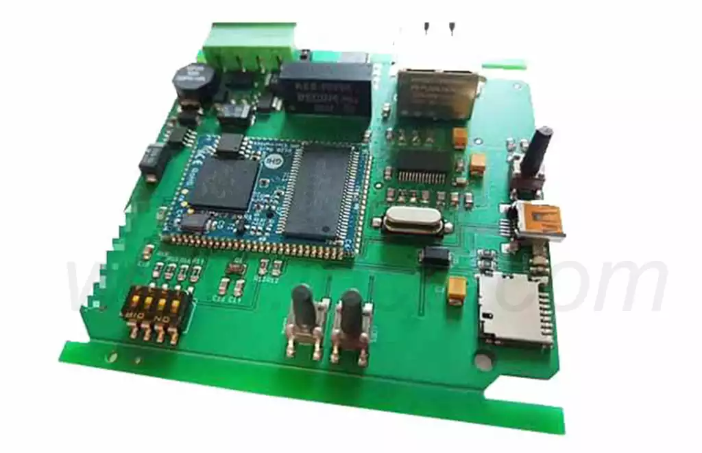
- Alumina ceramic substrate production process, alumina ceramic substrate production process of important technical links
Drilling: Mechanical drilling is used to form a connecting tube between the metal layers;
Plated through-hole: after drilling the copper wire between the connecting layers, the interlayer circuit is not open. Therefore, a conductive layer must be formed on the hole walls to connect the wires. This process is commonly referred to in the industry as “PTH” and consists of three main processes, slag removal, chemical copper plating and copper plating;
Dry-film pressing: to make photo-etched light-sensitive layer;
Outer layer exposure: after the light-sensitive film, the circuit board similar to the inner layer of the production process, again exposure, development. The main role of this photographic film is to determine the area that needs to be plated, and the area we cover is the area that does not need to be plated;
Magnetron sputtering; the use of positive ions generated during gas glow discharge and the exchange of energy and momentum between the atoms on the target surface to move the material from the source material to the substrate to achieve thin film deposition;
Etch formation of external lines: a technique that utilizes chemical reactions or physical impacts to remove material, the role of etching is reflected in the selective removal of specific patterns;
- Alumina ceramic substrate plating
Nickel plating on alumina pcb is divided into nickel plating and chemical nickel plating, while nickel plating is carried out in an electrolyte consisting of nickel salt (called the main salt), conductive salt, pH buffer and wetting agent.
The anode is nickel metal and the cathode is the plated part. A direct current is applied to deposit on the cathode (plated part). The upper layer is a uniform and dense nickel-plated layer. Nickel has good chemical stability in the atmosphere and in alkaline solutions and is not easily discolored.It is only oxidized when the temperature is higher than 600°C. It dissolves very slowly in sulfuric acid and hydrochloric acid, but is easily dissolved in dilute nitric acid. It is easy to passivate in concentrated nitric acid, so it has good corrosion resistance. Nickel plating is hard, easy to polish, and has high light reflectivity, which increases its appearance. The disadvantage is that it has porosity.
The main task is to completely strip the plating resist and expose the copper to be etched to the etching solution. Since the top of the wiring area is already protected by tin, the copper is etched using an alkaline etching solution, but since the wiring is already protected by tin, it can be kept in place so that the wiring in the wiring area provides an integral terminal block.
Alumina pcb has good electrical conductivity, mechanical strength and high temperature resistance. It should be noted that ultrasonic cleaning is required. Alumina ceramics are versatile ceramics, and due to their superior performance, their application in modern society is becoming increasingly widespread to meet the needs of daily use and special performance.