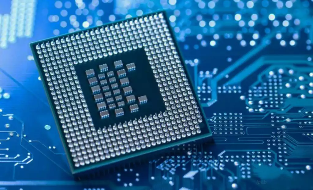
AOI, or Automatic Optical Inspection, is a device based on optical principles to detect common defects encountered in welding production.
AOI is a newly emerging new testing technology, but it is developing rapidly, and many manufacturers have introduced AOI test equipment. When AOI is used, the machine automatically scans the PCB with a camera, captures images, compares the tested solder joints with the qualified parameters in the database, and after image processing, checks for defects on the PCB substrate and displays/labels the defects through a monitor or an automatic sign for maintenance personnel to fix.
Automatic Optical Inspection Components
There are two basic components of an AOI system: the optical system and the software algorithms, which may vary depending on the manufacturing process.
Optical System in AOI
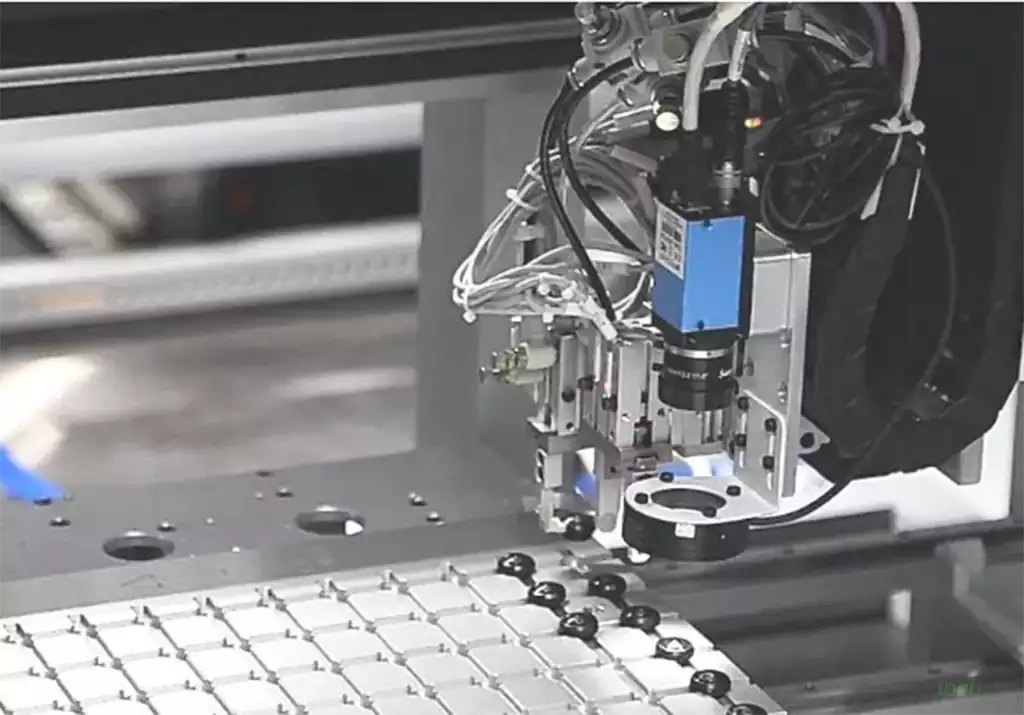
The optical system plays a key role in an AOI system because it is responsible for acquiring images of the items to be inspected. The quality of these images directly affects the overall performance of the system.A typical optical system in AOI consists of a light source, a set of lenses, and a digital camera.
Light Source: The light source illuminates the product being inspected. The type, color, and angle of illumination of the light source can greatly affect the effectiveness of defect detection. Different AOI systems use different types of light sources depending on the application. Previously, different light sources were used, such as fluorescent, incandescent and UV lamps. However, modern systems use LED arrays and halogen lamps to provide consistent and even illumination.
Lens: This component of the system directs light reflected from the product to the camera sensor. A high-quality lens is essential for capturing a clear image. The lens system can be adjusted to change the field of view and depth of field to be able to inspect different sizes and types of products.
Cameras: Finally, a digital camera takes an image of the product.Cameras in an AOI system range from standard 2D cameras to sophisticated 3D sensors that capture depth information.They contain millions of tiny photosensitive cells called pixels that convert the light they receive into digital data. AOI’s software algorithms then process that data to perform inspections.
Key features of AOI automated optical inspection systems
- High-efficiency inspection, not affected by circuit board placement density;For different inspection items, combined with optical imaging processing technology, respectively, there are different detection methods;Simple and user-friendly operation interface, no need for professionals to operate.
- Display the actual error image, convenient for the operator to carry out the final visual verification.
- Can count the NG data and analyze the causes of defects, real-time feedback process information to the operator.
In the PCBA chip processing, AOI technology is mainly used in the following several links:
- Pre-soldering inspection: Before welding, AOI technology can test the pins and pads of components to ensure that their size, shape and so on in line with the design requirements, to avoid welding defects caused by bad pins or pads.
- Post-soldering inspection: After the welding is completed, AOI technology can inspect the solder joints to identify whether there are defects such as false soldering, fake soldering, cold soldering, etc., and feedback the defective information to the operator for timely repair.
- Process monitoring: In the production process, AOI technology can monitor the welding quality in real time, and discover and deal with potential quality problems in time. This not only improves product quality, but also reduces rework and scrap rates and production costs.
Automatic Optical Inspection (AOI) technology plays an increasingly important role in the field of PCBA chip processing with its high efficiency and accuracy. In the future, with the continuous progress of technology and market demand changes, AOI technology will usher in a broader development prospects.