PCB laser processing is a manufacturing technique that employs high-energy-density laser beams to mark, cut, or drill holes in printed circuit boards (PCBs), finding extensive application within the electronics manufacturing sector.
PCB laser processing is a manufacturing technique that employs high-energy-density laser beams to mark, cut, or drill holes in printed circuit boards (PCBs), finding extensive application within the electronics manufacturing sector.
Primary Applications and Principles of PCB Laser Processing:
Laser Marking
By locally irradiating the printed circuit board surface with a laser beam, the material’s surface layer undergoes vaporisation, discolouration, or chemical reactions to form permanent markings such as QR codes, text, or symbols. This technique offers high precision, clear markings, and anti-counterfeiting properties, resisting fading or wear from environmental factors.
Laser Drilling (Laser Drilling)
Utilises the high temperatures generated by a focused laser beam to instantly melt or vaporise PCB material, creating minute holes (e.g., blind holes, through-holes) for interlayer electrical connections or special design requirements. Laser drilling can process apertures as small as 50μm, achieving precision far exceeding traditional mechanical drilling. It is a critical process in High Density Interconnect (HDI) PCB manufacturing.
Laser Cutting
Utilises laser energy to cut printed circuit board materials into specific shapes or dimensions. Commonly employed for cutting flexible printed circuits (FPC), separating printed circuit board components, or trimming edges. As a non-contact process, laser cutting minimises mechanical stress on materials, making it suitable for thin, flexible, or complex-shaped circuit boards.
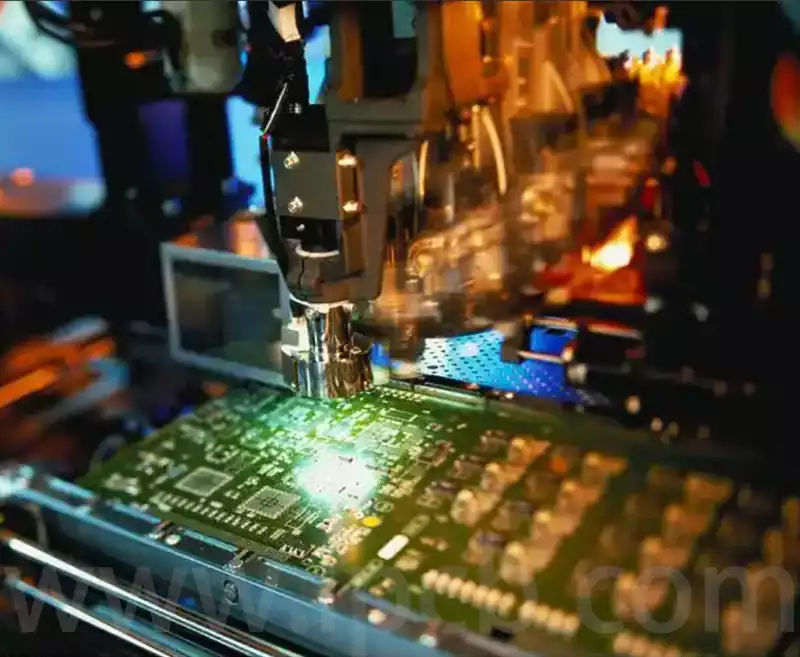
Principle: A laser beam generated by a laser source is focused onto the printed circuit board material via an optical system. Upon absorbing the laser energy, the material rapidly heats to its melting or boiling point, undergoing physical changes (such as melting or vaporisation) or chemical reactions to achieve marking, drilling, or cutting. Different laser types (e.g., CO₂ lasers, ultraviolet lasers) suit various materials and processing requirements. For instance, CO₂ lasers are suitable for organic materials, while ultraviolet lasers deliver excellent results on both metals and non-metals.
The Role of Laser Processing in Printed Circuit Boards
Enhanced Processing Precision: Laser technology offers distinct advantages in both high precision and high speed, enabling accurate processing of extremely minute areas on circuit boards. This characteristic is particularly crucial in the manufacturing of high-density, high-precision electronic circuit boards, effectively ensuring product quality and performance. For instance, in the production of smartphone motherboards, the achievement of minute line spacing and precise aperture processing relies on laser technology, guaranteeing the stable operation of various complex functions.
Enhanced Production Efficiency: Traditional printed circuit board processing methods involve lengthy cycles and complex workflows. The introduction of laser technology simplifies processing steps, significantly shortening production cycles and thereby markedly improving efficiency. For instance, in the mass production of tablet PC circuit boards, laser technology enables the processing of greater volumes within shorter timeframes, meeting the market’s demand for rapid supply.
Expanded Application Scope: Laser technology, with its high flexibility and versatility, can meet the processing demands of circuit boards of different types and specifications. Whether rigid or flexible circuit boards, laser technology enables efficient and precise processing. Within the wearable technology sector, flexible circuit boards require bending and folding to conform to device shapes. Laser technology enables precise cutting, drilling, and other operations on flexible substrates, ensuring printed circuit board performance remains unaffected.

Correct Usage Method
Equipment Selection and Commissioning: Selecting laser equipment that aligns with your production requirements is the primary step. During selection, key factors such as precision, speed, and stability must be comprehensively evaluated. Following installation, meticulous debugging and calibration must be conducted to ensure optimal operational condition. For instance, processing circuit boards for high-precision medical electronics necessitates selecting laser equipment with exceptional accuracy and adhering strictly to the operating manual during calibration to guarantee precise machining.
Material Pre-treatment: Thorough preparation precedes PCB processing. This involves surface cleaning to remove grease and contaminants. Depending on specific requirements, additional pre-treatment may be necessary, such as applying protective coatings. For automotive electronic PCBs, surfaces must be thoroughly cleaned to prevent dust and impurities from compromising precision, while protective coatings enhance corrosion resistance.
Process Parameter Configuration: Parameter settings are critical during laser processing. Key parameters such as laser power, scanning speed, and processing depth directly impact processing outcomes and product quality, necessitating precise adjustment and optimisation based on actual conditions. When processing high-frequency communication circuit boards, laser power and scanning speed must be accurately configured according to the board’s material and thickness to ensure the processed circuits meet high-frequency signal transmission requirements.
Process Monitoring: During laser processing, real-time monitoring of equipment operation and processing outcomes is essential. Utilising the equipment’s built-in monitoring systems or external detection devices enables timely identification and resolution of anomalies, ensuring uninterrupted processing. For instance, monitoring systems allow continuous observation of laser beam focus and processing depth; any deviations detected necessitate immediate parameter adjustments to maintain processing quality.
Post-Processing and Inspection: Following laser processing, printed circuit boards undergo post-processing and inspection. This encompasses removing processing residues, verifying processing outcomes, and conducting electrical performance tests. Rigorous post-processing and inspection protocols ensure the boards meet specified quality and performance standards. For aerospace electronic circuit boards, comprehensive electrical testing post-processing verifies stable operation under extreme environmental conditions.
Operational Precautions
Safety Protective Measures: The laser beam generated during laser processing poses potential hazards to human health. Operators must wear specialised protective eyewear and clothing at all times to prevent direct laser exposure to skin or eyes. When operating large-scale laser processing equipment, personnel must maintain full protective gear throughout the process to ensure personal safety.
Equipment Maintenance: Regular servicing of laser equipment is essential. This encompasses cleaning surfaces, inspecting component wear, and promptly replacing damaged parts. Proper maintenance extends equipment lifespan and preserves consistent processing performance. For instance, weekly lens cleaning and monthly transmission component inspections ensure operational reliability.
Processing Environment Control: PCB laser processing demands stringent environmental conditions. During operation, maintain a dry, well-ventilated indoor environment to prevent dust and impurities from interfering. This enhances processing quality and reduces defect rates. When performing printed circuit board laser processing in cleanrooms, strictly control air humidity and dust levels to ensure compliance with environmental requirements.
With micron-level precision and high-efficiency processing capabilities, printed circuit board laser technology has become a core driver for upgrading electronic manufacturing. Its applications span high-precision scenarios from smartphones to aerospace components, where standardised operation and continuous innovation are pivotal to unlocking its potential. Looking ahead, the deep integration of laser technology with intelligent control systems will propel PCB laser processing towards new heights of precision and intelligence in electronic manufacturing.


