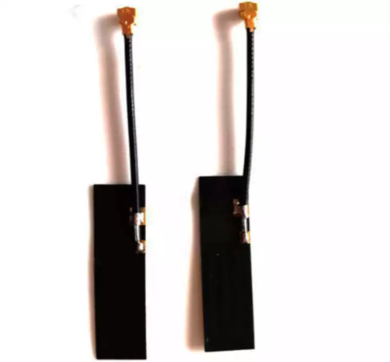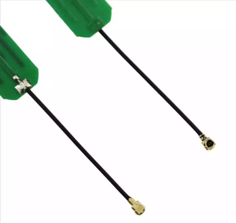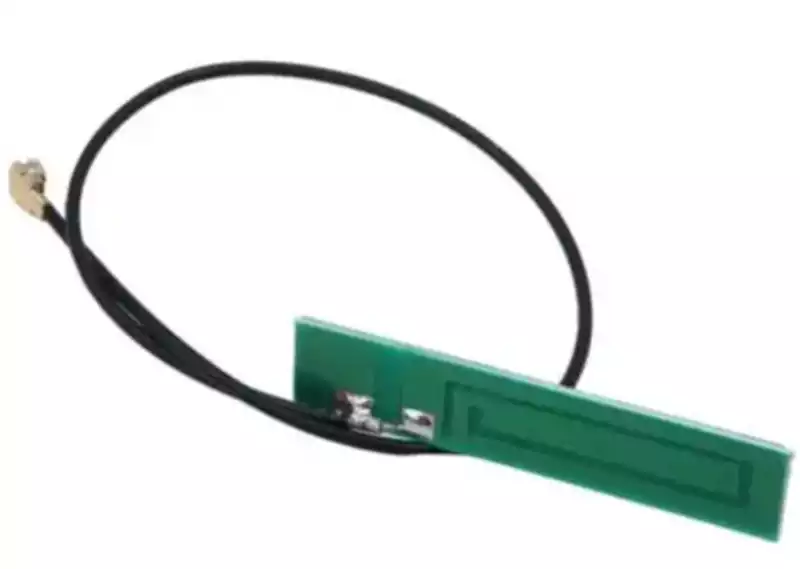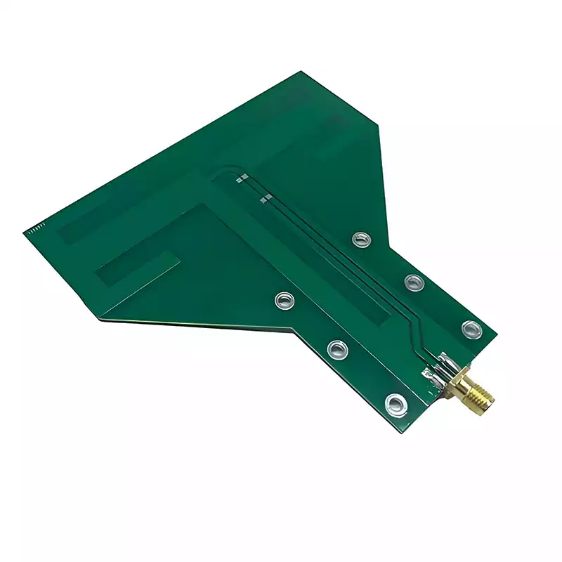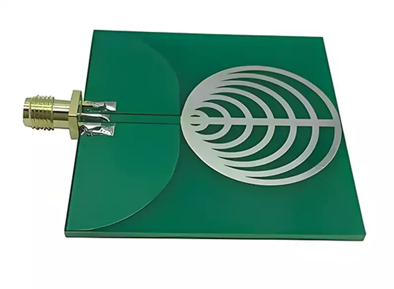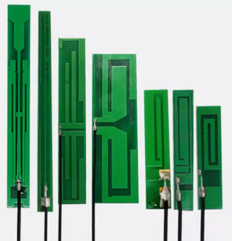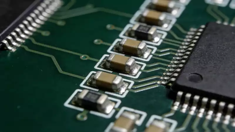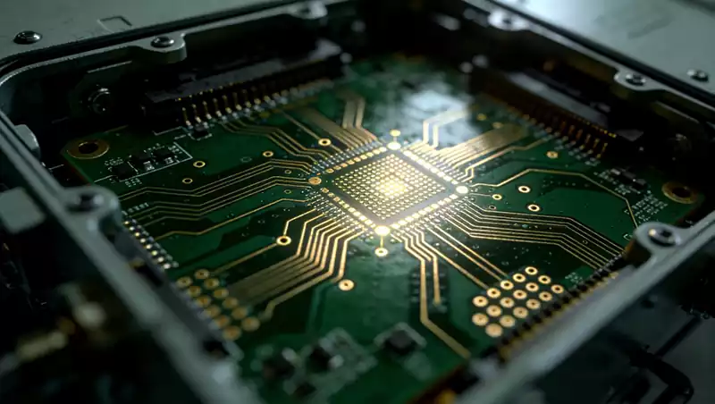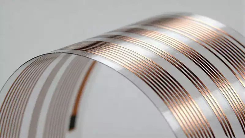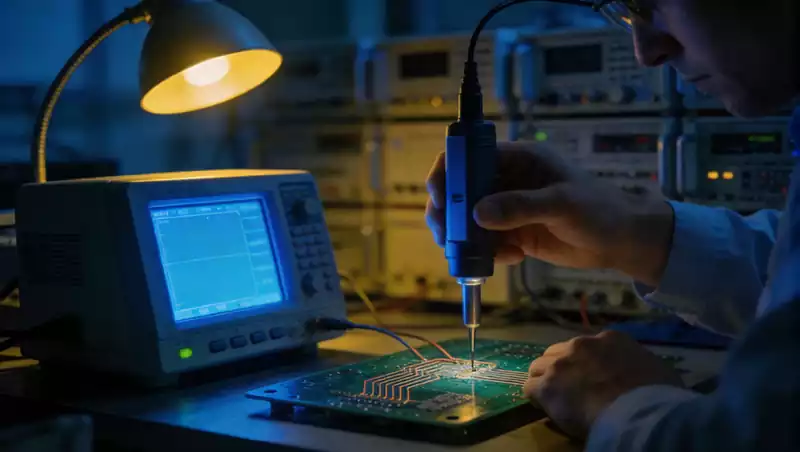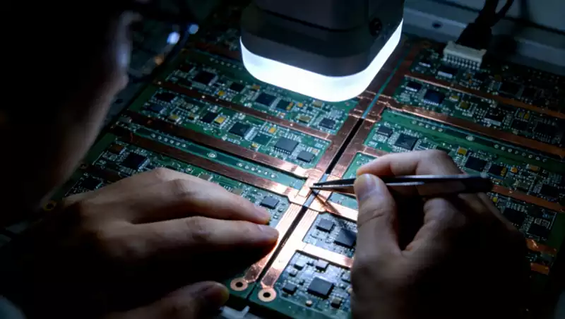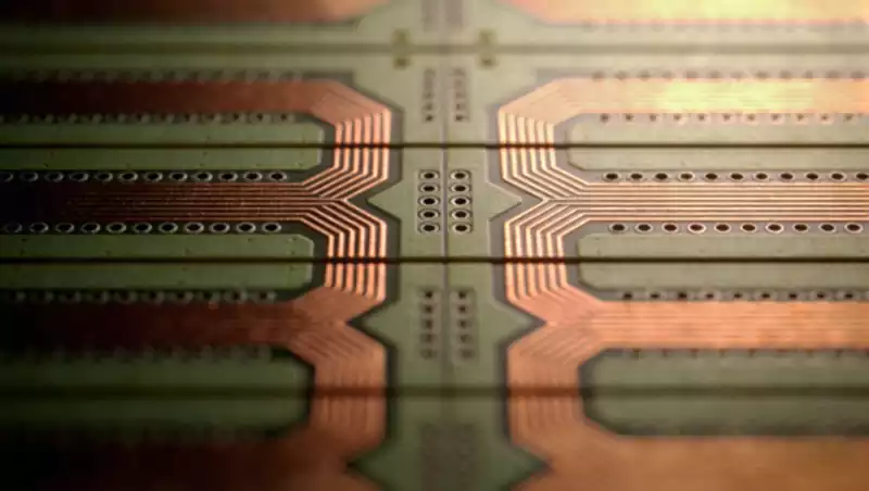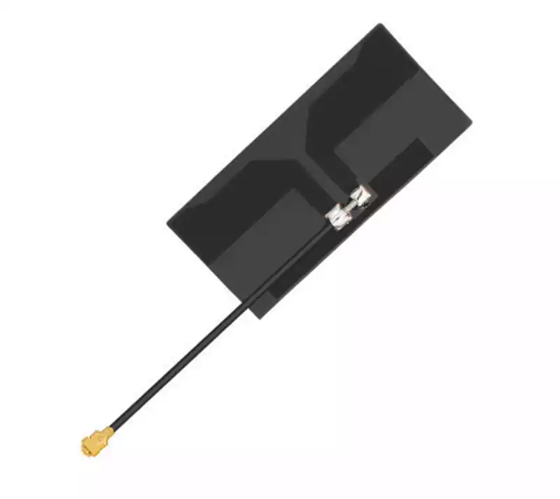
Assembly Challenges of Flexible Antennas
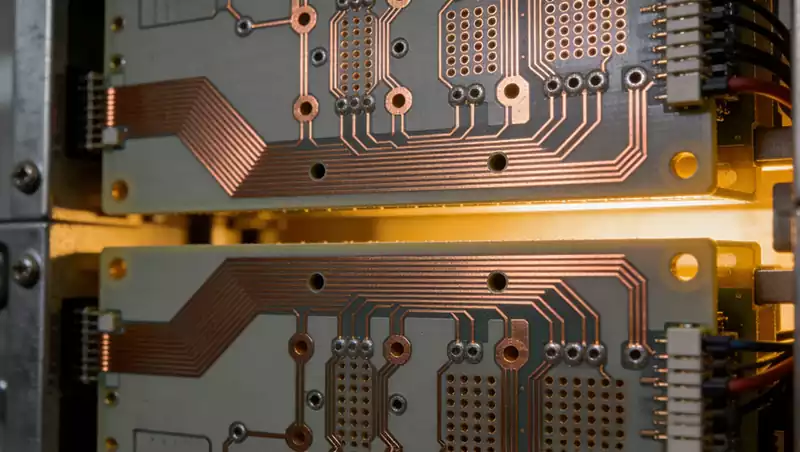
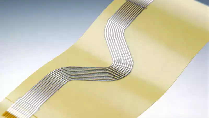
The fundamental challenge in assembling flexible antennas lies in the contradiction between “physical flexibility” and “assembly precision.” The substrate is extremely thin—almost paper-like—yet it must support micron-level alignment accuracy. The circuitry is delicate and flexible, yet it must maintain signal integrity across various operating conditions. Drawing on hands-on experience from the PCB manufacturing industry, we […]