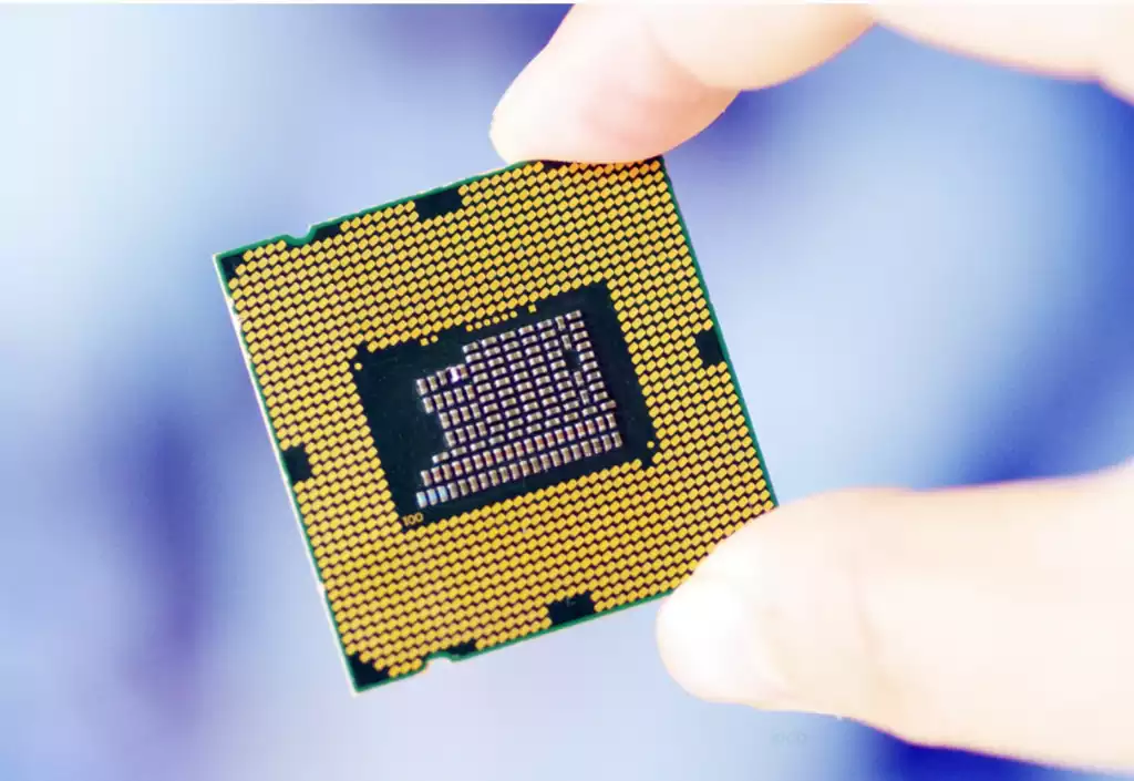
BGA technology (Ball Grid Array Package) that is the ball grid array packaging technology, is about the early 1990’s by the United States Motorola and Japan Citizen jointly developed high-performance packaging technology, BGA IC is in the back of the substrate according to the array way to make a ball contact as a pin, in the front of the substrate to assemble IC chips. BGA technology is the best choice for high-density, high-performance, multi-pin packaging of multi-pin large-scale IC chips. However, the BGA package occupies a large area of the substrate.
BGA technology is a surface adhesion technology applied to integrated circuits and is often used to permanently fix devices such as microprocessors. Its main functions include:
Improved integration: BGA provides more pins than other package types, allowing the entire bottom surface of the device to be used as pins instead of just the periphery, thus improving integration.
Optimized electrical performance: BGA packages have smaller size, better thermal performance and electrical performance, for example, BGA packages have a faster and more efficient way to dissipate heat compared to traditional TSOP package methods.
Improvement of memory capacity: Memory packaged with BGA technology can increase memory capacity by two to three times with the same memory size.
Improve signal transmission: The I/O terminals of BGA package are distributed underneath the package in the form of round or columnar solder joints in an array, which makes the signal transmission delay small and the frequency of use much higher.
Improved reliability: BGA technology assemblies can be coplanar soldered for high reliability.
The thickness and weight of BGA technology are reduced compared to previous packaging technology, reducing parasitic parameters and providing excellent stability. However, there are still some problems with BGA packages, such as high substrate costs and warpage problems with plastic BGA packages.
Overall, the role of BGA technology is mainly in improving integration, optimizing electrical performance, enhancing storage capacity, improving signal transmission and improving reliability.
There are various types of BGA (Ball Grid Array) technology, and the following are some common classifications:
Categorized by the way the solder balls are arranged:
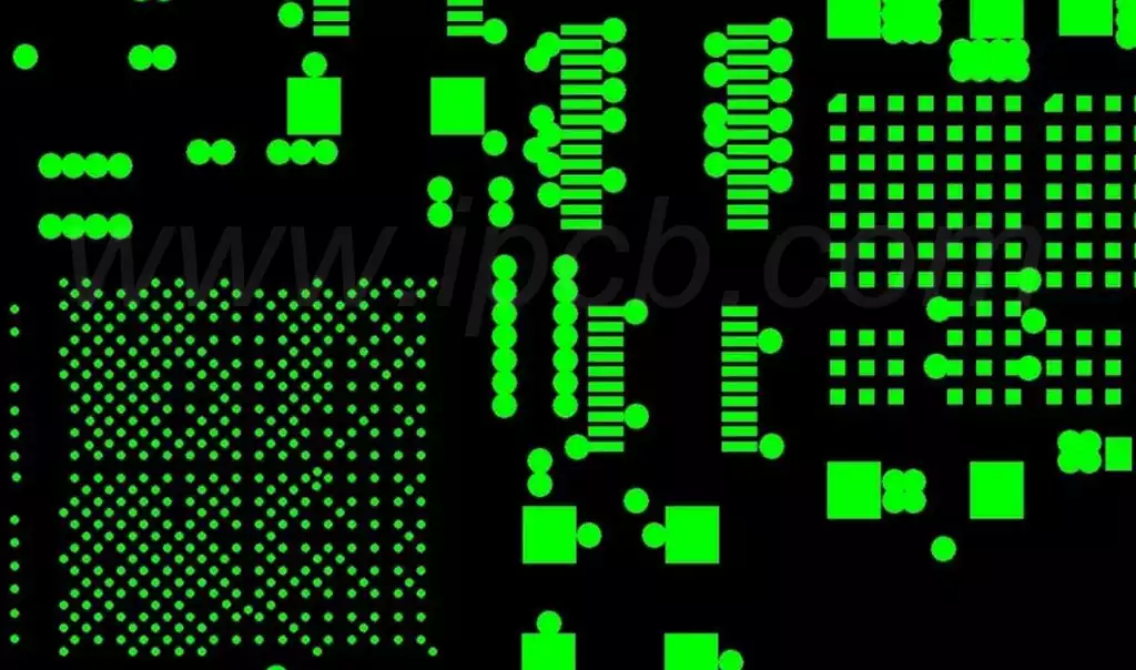
Peripheral BGA (Peripheral BGA): The solder balls are distributed around the chip, and are only connected at the bottom of the chip.
Interstitial BGA (Interstitial BGA): solder balls are interleaved around the chip to provide better connectivity.
Full-array BGA (Full-array BGA): the solder balls are fully covered at the bottom of the chip, providing better connectivity.
Categorized by substrate type:
PBGA (Plastic BGA): Using plastic as the substrate, it is the most common type of BGA.
CBGA(Ceramic BGA): Using ceramic as the substrate, it has better heat resistance and electrical performance.
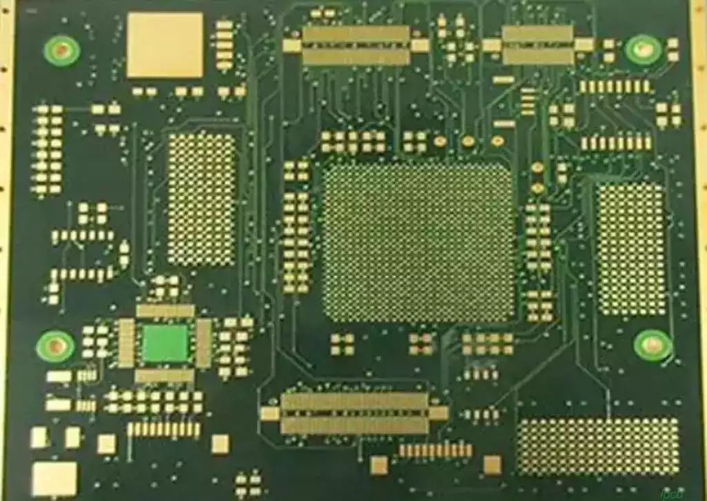
FCBGA(Flipchip BGA): Also known as Flipchip BGA, the soldering point of the chip is on the other side of the PCB substrate, which has higher integration.
TBGA (Tape BGA): Also known as tape-carrying BGAs, they use film or other flexible materials as the substrate and are suitable for miniaturization and lightweight applications.
BGA IC Package Advantages
- BGA packages have very few external components, nothing but the chip itself, some interconnect wires, a very thin substrate, and a molded cover. There are no very large pins and no lead frame. The height of the entire chip on the PCB can be 1.2 millimeters.
- Signal transmission delay is small, adapt to the frequency is greatly improved
- Efficiently design out the distribution of power and ground pins. Ground bounce effect also because the number of power and ground pins is almost proportionally reduced.
- Most BGA packages have large pads for easy handling. Flip chip assembly requires stress relieving of the soldered seams again in order to prolong thermal aging and cycle life.
- BGA package is very secure, with 20 mil pitch QFP compared to BGA can not be bent and broken pins are very secure.
- Advanced BGA package, you can put all the pins are placed right under the chip, not more than the chip package, which is good for miniaturization.
The number of I/O pins is increased, but the distance between the pins is much greater than the QFP package method, which improves the yield.
BGA IC technology, as a major innovation in the field of IC packaging, has become an indispensable packaging technology in the manufacture of modern electronic devices since its birth in the early 1990s, by virtue of its high-density, high-performance, multi-pin and other characteristics. It will continue to play an important role in the field of IC packaging as electronic technology advances and consumer demand increases.