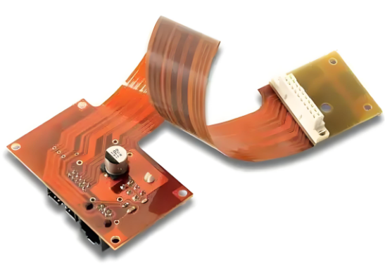
BGA (Ball Grid Array) package, or Ball Grid Array package, is an array of solder balls on the bottom of the package substrate to serve as the I/O terminals of the circuits to be interconnected with the printed circuit board (PCB). Devices packaged with this technology are surface mount devices.
BGA packaging classification
- PBGA (Plastic BGA) substrate: generally 2-4 layers of organic material composed of multi-layer boards. Intel series CPU, Pentium II, III, IV processors are used in this packaging form. In the last two years, there is another form: the IC is directly bound to the board, its price is much cheaper than the regular price, generally used in the quality requirements of the game is not strict and other areas.
- CBGA (CeramicBGA) substrate: that is, ceramic substrate, the electrical connection between the chip and the substrate usually adopts the FlipChip (FC) installation method. Intel series CPUs, Pentium I, II, Pentium Pro processors have used this packaging form.
- FCBGA (FilpChipBGA) substrate: rigid multi-layer substrate.
- TBGA (TapeBGA) substrate: the substrate is a strip of soft 1-2 layers of PCB circuit boards.
- CDPBGA (Carity Down PBGA) substrate: refers to the center of the package has a square-shaped low-slung wafer area (also known as the cavity area)
Advantages of BGA package
- BGA volume is small, large memory capacity, the same memory IC in the same amount of capacity, BGA volume is only one-third of the SOP package.
- The pins of QFP and SOP package are distributed around the body, when the pins are many, the spacing is reduced to a certain extent, the pins are easy to deform and bend, but the BGA solder ball is at the bottom of the package, the spacing is increased, which greatly improves the yield rate.
- Good electrical performance, BGA pins are very short, using tin balls instead of wires, the signal path is short. This reduces the inductance and capacitance of the lead wires and enhances the electrical performance.
- Good heat dissipation, spherical contact array and the substrate contact surface to form a gap, which is conducive to the body heat dissipation.
- BGA body and PCB board has good coplanarity, can effectively guarantee the welding quality.
Disadvantages of BGA packaging
- After BGA welding quality inspection and maintenance is difficult, must use X-Ray fluoroscopy to ensure the electrical performance of the welding connection. It is impossible to determine the inspection quality by naked eye and AOI.
- BGA pins in the body of the bottom, easy to cause the welding shadow effect, the temperature curve of the food on the welding of higher requirements. It is necessary to monitor the actual temperature of welding.
- BGA pin individual soldering defects, the entire BGA must be removed to replant the ball, and then the second patch welding. This affects the through rate and electrical performance.
- BGA packaging is very reliable, compared with the 20 mil pitch QFP, BGA can not be bent and broken pins. Soldering is secure, generally if you want to remove the BGA package, you must use the BGA rework station to remove the high temperature to be able to complete.
BGA soldering voids are the phenomenon of voids in BGA solder joints. These voids may be due to moisture in the material and organic matter in the solder paste that generates gases through high temperatures during the soldering process, and when these gases cannot be expelled efficiently, they are surrounded by the alloy powder to form voids.BGA solder voids affect the mechanical and electrical properties of the solder joints, such as decreasing the strength, ductility, creep, and fatigue life of the joints, and they can also form hot spots that can reduce the reliability of the joints.
BGA solder voids are most commonly found at the component level, which is the portion of the solder ball between the center of the ball and the BGA substrate. This can be due to the presence of air bubbles and volatile flux gases in the BGA pads on top of the PCB during the BGA reflow soldering process, forming voids when the eutectic solder balls of the BGA and the applied solder paste fuse together during the reflow process. If the reflow temperature profile in the reflow zone time is not long enough, air bubbles and flux volatile gases can not escape in time, the molten solder has entered the cooling zone into a solid state, the formation of voids.
In order to reduce the formation of BGA soldering voids, you can use lead-free solder paste for soldering, because lead-free solder paste can effectively reduce the formation of voids. In addition, reducing the use of organic substances is also an effective way to reduce the generation of voids. When soldering, it is necessary to combine the surface tension of the solder paste, the component’s own gravity and other factors to analyze why the gas can not escape from the surface of the alloy powder, and thus the formation of voids.

Solder voids in BGA technology can have an impact on the mechanical and electrical properties of the solder joint.
On the one hand, the location of a solder cavity is a stress concentration point, which affects the mechanical properties of the solder joint and reduces the strength, ductility, creep and fatigue life of the joint. At the same time, weld voids can also form excessive hot spots, reducing the reliability of the welded joint.
On the other hand, some viewpoints believe that voids can abort the expansion of cracks in solder joints and have an inhibitory effect on the spread of cracks.
Therefore, the impact of soldering voids in BGA technology has two sides, and its specific impact depends on the specifics of the voids.
Solve the problem of soldering voids in BGA can be started from the following aspects:
Solder paste activity: choose a more active solder paste, its ability to remove oxides is stronger, which is conducive to reducing the rate of voids.
Component baking: baking before using pcb components can remove the water vapor in the components and reduce the void rate.
Curve setting: According to the characteristics of the solder paste, adjust the furnace temperature curve, appropriately extend the holding zone time, so that the gas has enough time to eliminate, thus reducing the void rate.
Component package form: for DPAK components at the bottom of the pad is large and easy to cause the problem of large voids, you can start from the pad design and stencil design to improve.
Flux paste performance: Select the appropriate flux paste to ensure its ability to wet the pad, reduce surface tension, and control the content of non-volatile substances.
Rosin Selection: For BGA flux paste, it may be more appropriate to select a rosin with a low softening point.