The body to body clearance for smt parts is the minimum distance that must be maintained between two neighboring components in surface mount technology (SMT). This distance is required to ensure board performance and reliability while avoiding electromagnetic interference and thermal conduction problems.
Minimum body to body clearance for smt parts Standard
IPC-7351B is an industry standard widely used in SMT circuit design, which provides some recommended values for the minimum body to body clearance for smt parts. According to this standard, in general, the minimum body to body clearance for smt parts should be between 0.5mm and 1mm. For some special cases, such as high-frequency circuits or high-voltage circuits, the component spacing may need to be increased.
(1) For normal SMT placement density, the minimum body to body clearance for smt parts shall be in accordance with the requirements shown in the figure, which applies to the component layout density of general PCB assembly.
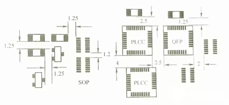
① Between chip components, between SOTs, and between SOICs and chip components is 1.25mm.
② Between SOIC, 2mm between SOIC and QFP.
③ 2.5mm between PLCC and chip components, SOIC and QFP
④ 4mm between PLCCs
⑤ Care should be taken when designing PLCC sockets to allow for the size of the PLCC socket (the pins of the PLCC are on the inside of the bottom of the socket)
(2) Minimum body to body clearance for smt parts between SMC/SMD and through-hole components:The minimum spacing between SMC/SMD and through-hole components when mixing smt patch is determined according to the package size of the through-hole components. The main consideration is the shape of the package body and the height of the component body, the minimum distance between the cartridge components and sheet components is generally more than 1.27mm.
(3) high-density pcb assembly pad body to body clearance for smt parts
: the current 0201 pcb pad spacing is generally 0.15mm, the minimum spacing of 0.10mm; 01005 minimum spacing of 0.08mm.
Common body to body clearance for smt parts design basis include:
Stencil flaring requirements
Especially for components with poor pin coplanarity, such as transformers, the space design of stencil flare must be considered.
Appropriate redundancy in spacing
During the SMT placement process, sufficient spcing spcae needs to be reserved for placement machine operation and rework, including the operating space required for BGA rework, manual soldering, power-on test and ICT test processes.
Quality Control Requirements
Component spacing design needs to ensure the quality of the SMT placement process, to ensure that the solder paste is well printed and the placement process to avoid solder bridging and other defects due to the proximity of the spacing caused by the bridge.
The body to body clearance for smt parts is usually affected by the following factors.
Component size and type: The minimum body to body clearance for smt parts requirement may vary for different sizes and types of components. For example, the minimum pitch of a large component may be greater than the minimum pitch of a small component.
Production process: SMT production process of some process parameters, such as the accuracy of the placement machine, the nature of the paste, the temperature profile of the reflow soldering, etc., will affect the choice of component spacing.
Circuit design:Some parameters in circuit design, such as current density and voltage, will also have an impact on the component spacing requirements. High current density and high voltage may require greater component spacing to prevent arc discharge and electromagnetic interference.
Environment: The environment in which the components are used, such as ambient temperature, humidity, pressure, etc., will also have an impact on the component spacing requirements.
Why must there be a body to body clearance for smt parts?
- To prevent “solder run” short circuit production, the solder is “printed” through the stencil to the circuit board. If the hole in the stencil is too large, the stencil is too thick, or the stencil is loose and uneven, the solder will easily “run off”. For example, the 0402 size of the small resistance capacitance, the pitch is originally small, the solder is crooked, it is easy to connect the two components, resulting in a short circuit. Like squeezing the subway when there are too many people, everyone is squeezed to stick together and can not move.
- to the workers and machines “to stay alive,” whether it is a worker hand soldering, or with the machine patch, repair, there must be a place to start! If the components are too close to each other, the workers take the soldering iron when welding, accidentally will be hot next to the components; return to repair when you want to dismantle a large chip, the results of the side of the densely packed all the small components, simply can not be operated. This is like moving a large box in a narrow aisle, turn around are difficult.
- Solder pad design “pit” you some components of the pad if not well designed, the solder melting will climb up the side of the components. The thinner the component, the more powerful climb, and finally the two components “sticky” together. For example, 0.3mm pitch of the small chip, if the pad is a short cut, the welding will be easy to “turn over”.
- Different factories “craft” is not the same as some factories have advanced equipment, patch precision can reach 0.1mm, some factories may only guarantee 0.3mm error. So the design pitch can not be a one-size-fits-all, depending on the actual level of the factory. Now there is specialized software to help detect, red means “danger! Hurry up and change”, yellow is ‘a little suspended, look again’, green is ‘safe through’.
Possible problems with small body to body clearance for smt parts
The distance between components is often an important consideration in the circuit design and layout process. If the distance between components is too small, it may adversely affect circuit stability and reliability.
- Potential Short Circuit Problems
A small distance between components may create a potential short circuit risk. When the distance between two components is not sufficient to withstand the voltage or current, a short-circuit failure may result. In addition, if the component terminals are too close to each other, it can also cause misconnections and poor connections, which can lead to short-circuit situations. - Noise interference
A small distance between components may lead to electromagnetic interference and noise problems. When the distance between two components is too close, the phenomenon of mutual interaction may occur between them, thus creating the problem of mutual signal interference. This interference can adversely affect the performance and reliability of the circuit. - Difficult to return to repair
Connector “paste paste” connectors are generally higher components, in the layout of the time distance is too close to each other, assembled next to each other after the spacing is too small, does not have the returnability.
Reasonable design of body to body clearance for smt parts is to ensure the performance of the board and the key to production quality. Appropriate spacing not only to prevent welding short circuit and mechanical damage, but also effectively reduce electromagnetic interference and improve overall reliability. At the same time, reserving enough space helps subsequent overhaul and maintenance, and improves production efficiency. Comprehensive consideration of design specifications, process capabilities and the use of the environment in order to achieve high-quality PCB assembly and stable operation.