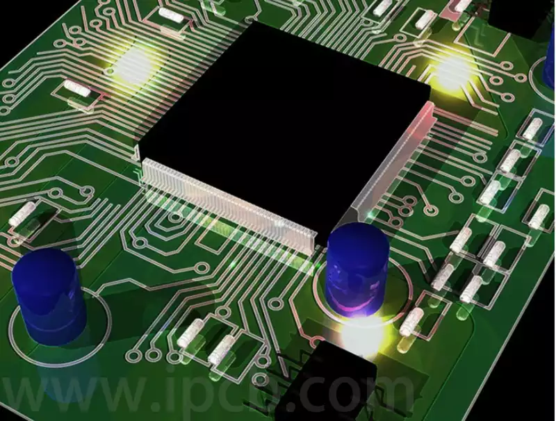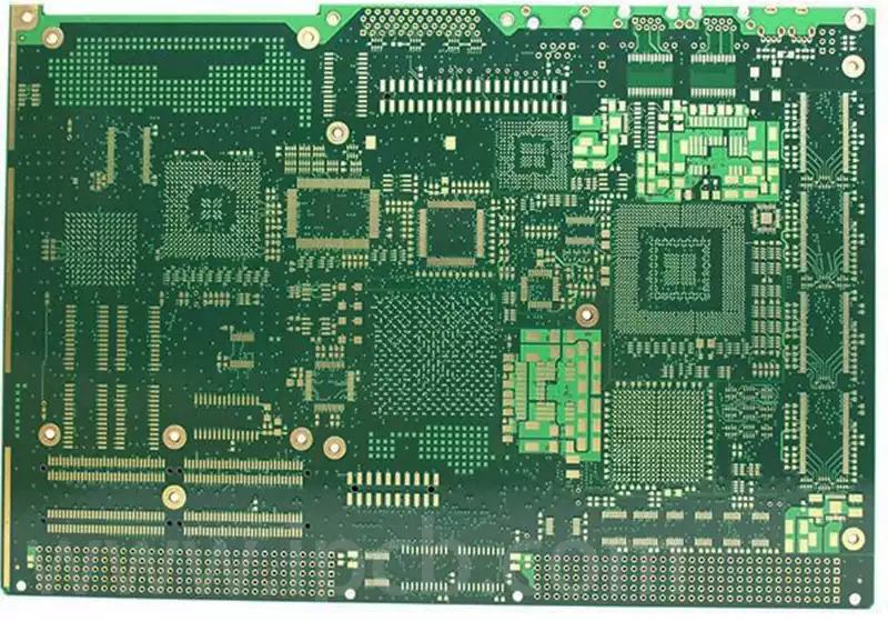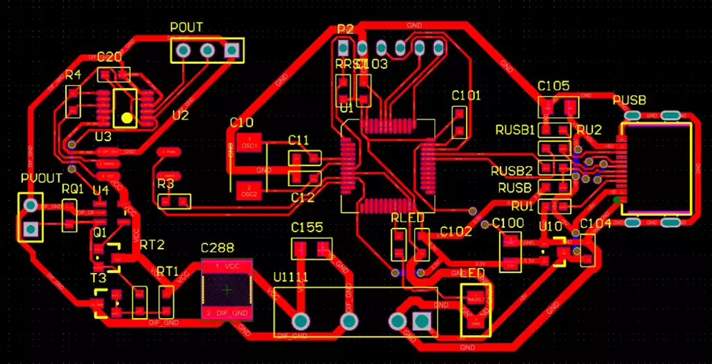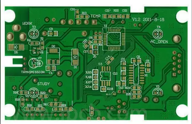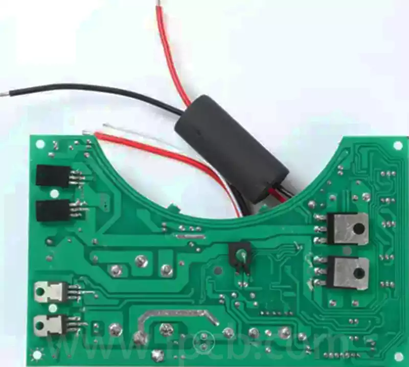
Differences between automotive circuit boards and ordinary
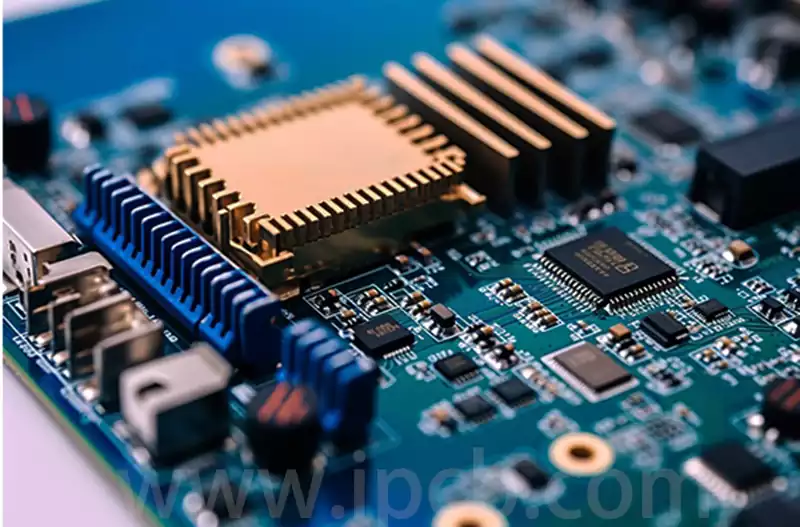
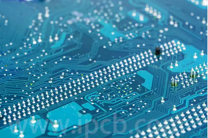
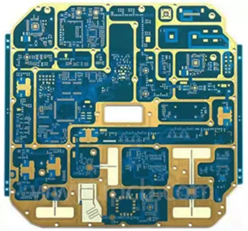
Automotive circuit board, full name of automotive printed circuit board, is a kind of electronic products using printing technology to print the copper foil line on the insulated substrate. It connects various electronic components such as resistors, capacitors, chips, etc. together through specific circuit patterns to achieve the transmission and processing of electronic signals, thus […]