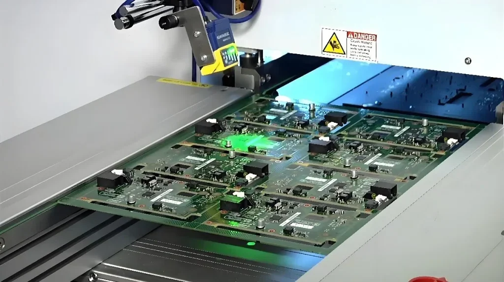
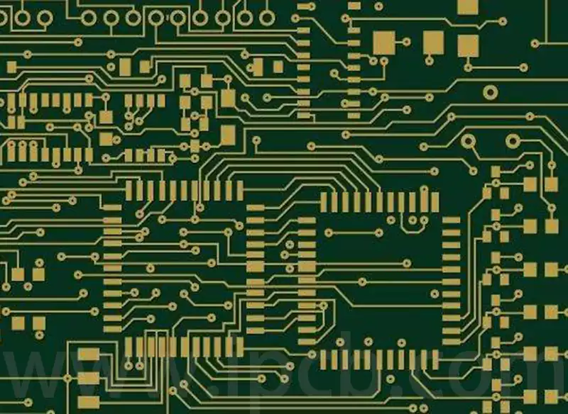
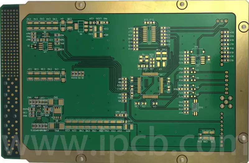
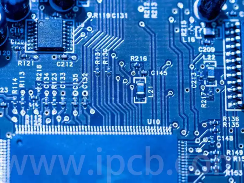
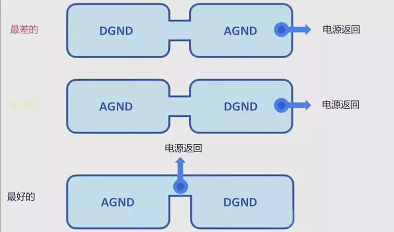
Technology Blog

Understanding PCB Circuits from Principles and Features

Principle and characteristic of PCB circuits

PCB is the abbreviation of Printed Circuit Board. Also known as printed circuit board or printed circuit board. it is called a “printed” circuit board because it is made using electronic printing. A printed circuit board is a substrate used for assembling electronic components. 1. Printed circuit board (PCB) It is a printed board that […]

free-pcb-layout-program

The best choice of free pcb layout program

In the field of electronic design, PCB layout is a crucial part. For beginners, how to quickly and accurately complete the PCB board layout is a major challenge. Fortunately, there are many free PCB layout program on the market, these tools are not only powerful, but also easy to get started, for electronic design beginners

wave-soldering

Wave soldering welding technology

Wave soldering refers to the molten brazing material, by electric pump or electromagnetic pump jet into the design requirements of the solder crest, can also be formed by injecting nitrogen into the solder pool, so that the pre-loaded components of the printed circuit board through the solder crest, in the brazing material surface to form

PCB-dielectric-constant

The PCB dielectric constant and performance requirements

The dielectric constant is an indicator of a material’s capacitive properties in an electric field, and it measures a material’s ability to store charge in an electric field. For PCB boards, the pcb dielectric constant DK value reflects the capacitance capability of the insulating layer of the board and is used to define the electrical

PCB protective coating

How to clean flux residue is a critical step in soldering

Flux is a chemical substance that removes oxides or other contaminants from the surface of the PCB, the solder itself, wets the metal surface to be soldered, protects the metal surface from re-oxidizing while soldering, reduces the surface tension of the molten solder, and facilitates the expansion and flow of the solder. However, once the

soldering-cold-jiont

The soldering cold joint phenomenon and prevention of pcb

Soldering cold joint is due to circuit board SMT processing in the reflow soldering process, the solder at the solder does not reach its melting point temperature or welding heat is not enough, so that in the wetting or flow before the solidification, not to form any metal alloy layer, so that all or part

pcb-thickness

PCB Thickness:A Balanced Choice for Performance and Cost

PCB thickness generally refers to the total thickness of the entire board,including the substrate (e.g., FR-4, etc.) and the thickness of the copper foil on two or more sides. The “copper thickness” refers to the thickness of the copper foil on one or both sides of the board,commonly measured in ounces (oz) or microns (μm).

pcb-board-connector

PCB board connector is a solid bridge in electronic circuit

A pcb board connector is a connection system mounted on a printed circuit board.PCB connectors are typically used to transfer signals or power from one PCB to another, or from another source in the structure of a device to or from a PCB. Since PCBs are not hardwired to each other and can be assembled

The exclusive way to understand PCB circuit boards

The exclusive way to understand PCB circuit boards

PCB circuit board is an indispensable component of modern electronic equipment. It is based on strong fiberglass and coated with one or more thin layers of copper foil to connect and support electronic components. Part 1: Basic knowledge of PCB circuit boards Before we dive into the design aspects of PCB circuit boards, let’s first

wafer-testing

Wafer Testing is a critical step

Wafer testing is for each grain on the wafer for needle test, in the detection head mounted on a gold wire made of fine as a hair of the probe, and the contact on the grain to contact, test its electrical characteristics, unqualified grains will be marked,and then when the wafer according to the grain

single-ground-point

The Analysis of pcb single point grounding strategy

Single point grounding means that there is only one physical point in the entire circuit system that is defined as the ground reference point, and all other points that need to be grounded are connected directly to this point. In low-frequency circuits, there is not much influence between wiring and components. Usually circuits with frequencies

pfc circuit

The Active PFC circuits with the gate drive optimization

To build passive power factor correction (PFC) circuits, we have traditionally relied on passive components such as capacitors and inductors to extend the current conduction angle and smooth the pulse to reduce harmonic distortion of the current. While this approach is simple and reliable, the size and cost issues of passive components come to the

370hr

370 HR Properties of the material

“370 hr” is a common PCB material type, which is a high-performance epoxy resin matrix commonly used to manufacture electronic equipment that requires high-temperature and high-frequency performance, such as high-speed communication equipment or aerospace equipment. This material has good thermal stability and mechanical properties, making it suitable for complex circuit designs. It has an important

splicing-boards

Explanation and practice of splicing boards technology

Splicing boards is the process of laying out multiple circuit boards on a single large size board to form an overall board assembly. The purpose of it is to maximize the use of board space, increase productivity and reduce costs. Methods of splicing boards1.V-CUTV-CUT is to draw a slot in the connection of two boards,

vcc

VCC is the Heart of Circuit Stabilization and Overhaul

VCC is a common term in circuits that means positive supply voltage. In digital or analog circuits, developers often need a widely available power supply to ensure that the circuit can operate properly. In such cases, the VCC voltage is usually set to a fixed value, such as 5V or 3V, so that all devices

pcba-number

PCBA Number: Ensuring Quality and Traceability

What is pcba number?PCBA number (or SN code) is a unique code used to identify and track product information on PCBA (Printed Circuit Board Assembly) boards. This code is labeled when the PCBA semi-finished product is put into production. The purpose of this code is to facilitate the traceability of the production process of the

PCB-antenna

PCB antenna is a efficient choice for wireless communication

PCB antenna, also known as printed circuit board antenna, is a form of antenna in which the antenna is printed directly on a PCB (printed circuit board). This type of antenna plays an increasingly important role in modern wireless communication devices, especially in mobile devices, IoT devices and wireless sensor networks, where it is widely

siliver-plating

PCB Silver Plating:Choice for Performance and Reliability

PCB silver plating technology refers to the PCB surface covered with a layer of silver metal process. Silver as an excellent conductive material, with good conductivity, oxidation resistance, thermal conductivity and other characteristics. Through the silver-plated processing, PCB conductivity has been significantly improved, while enhancing its oxidation resistance and thermal stability, thereby improving the performance

What is GND in electronic circuit

GND in Circuits: Understanding and Classifying

“GND” stands for “ground” in electronic circuits, and is the abbreviation of “Ground”. It can also be called zero point or system ground. It usually connects other components in the circuit to the ground potential to form part of the circuit. Ground is the reference point in the circuit. Its potential is zero relative to

pcb-wiring

The rules and performance guarantees of PCB Wiring

PCB wiring is a critical step in PCB design, which determines the performance and reliability of the product. It refers to the process of rationally laying out and connecting wires, components, etc. on a circuit board when manufacturing a printed circuit board (Printed Circuit Board, or PCB for short). This process needs to follow certain

pcb-cnc

PCB CNC milling machine technology overview

PCB CNC milling machine is an advanced point-to-point motion control system, which plays a key role in manufacturing high-precision printed circuit board through-hole. With the gradual miniaturization and refinement of electronic products, the printed circuit board conductive holes in the aperture, line width and line spacing requirements have become more stringent. Accordingly, PCB CNC system

pcb-copy-boarda

The copying and innovation of PCB copy board

What is pcb copy board?PCB copy board is a technical means, through the other people’s PCB samples for measurement, analysis and imitation, to complete the original product replication and improvement.It is widely used in the development and production of electronic equipment.PCB copy board is divided into hardware copy board and software copy board. It is

How to mounting holes on pcb boards

How to mounting holes on PCB boards

Mounting holes refers to the holes used to install the circuit board in PCB. These holes are usually located in the four corners of the PCB or along the edge, and are used to fix the position of the circuit board in the device, as well as to connect to the mechanical bracket or fixture

pcb-reflow-plate

pcb reflow plate: the cornerstone of PCB soldering

PCB reflow plate, also known as reflow board or thermal reflow board, is an auxiliary tool in the PCB manufacturing process. Its main function is to remove the solder paste or soldering material from the surface of the PCB’s pads evenly and quickly through the process of heating and cooling during the soldering process to

Scroll to Top