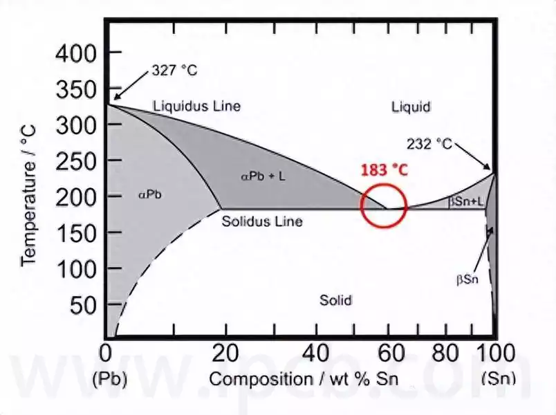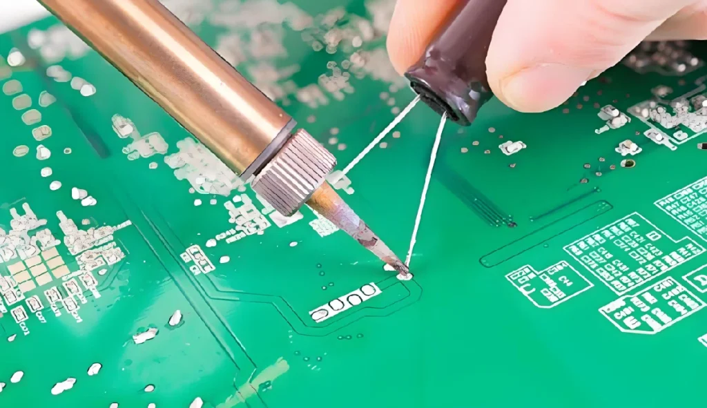
Exploring the Future of Solder Mask Material in PCB Design
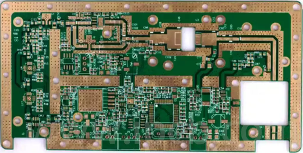
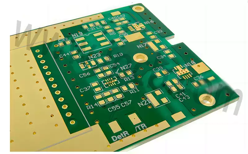
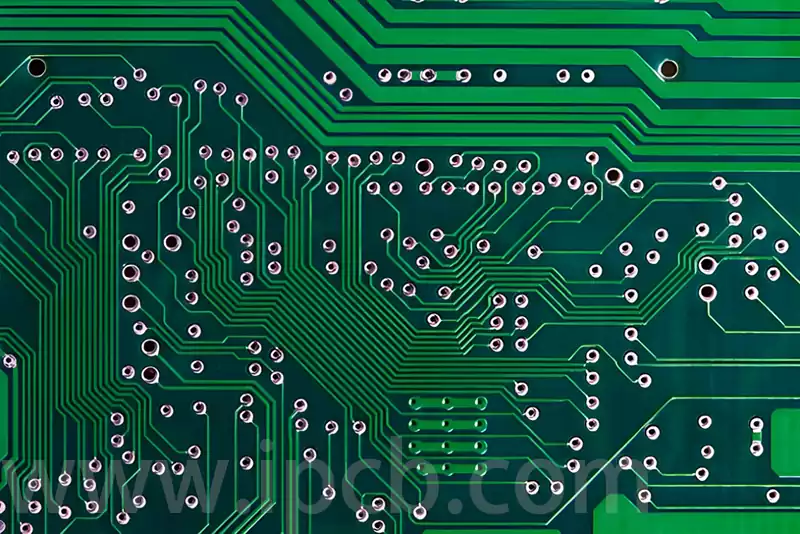
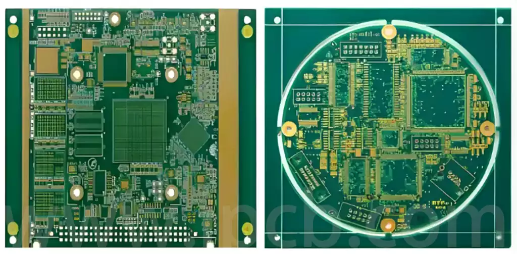
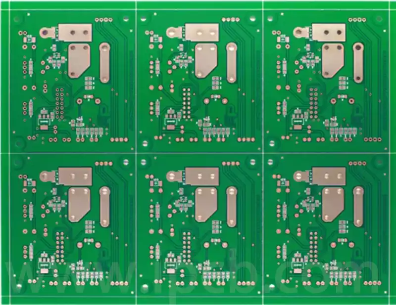
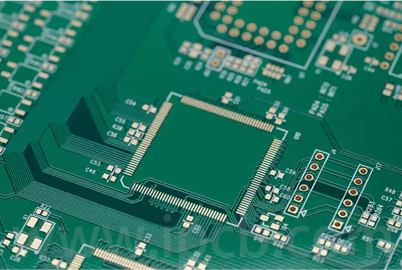
Definition and Function of Solder Mask Material in PCB Design In the printed circuit board (PCB) manufacturing process, solder mask is a crucial protective coating. It’s typically green, hence the nickname “green board,” but PCBs can also come in red, blue, black, white, and other colors. The solder mask material not only impacts the board’s […]