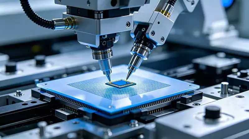
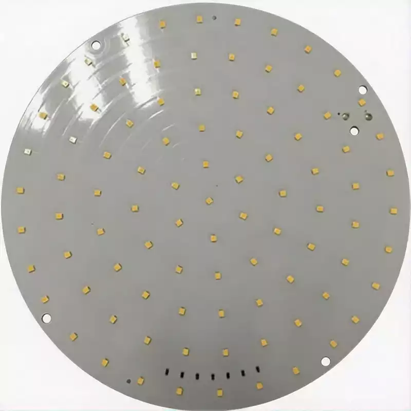
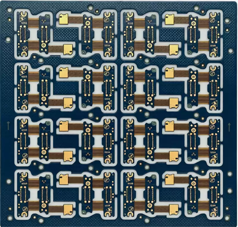
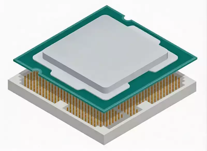
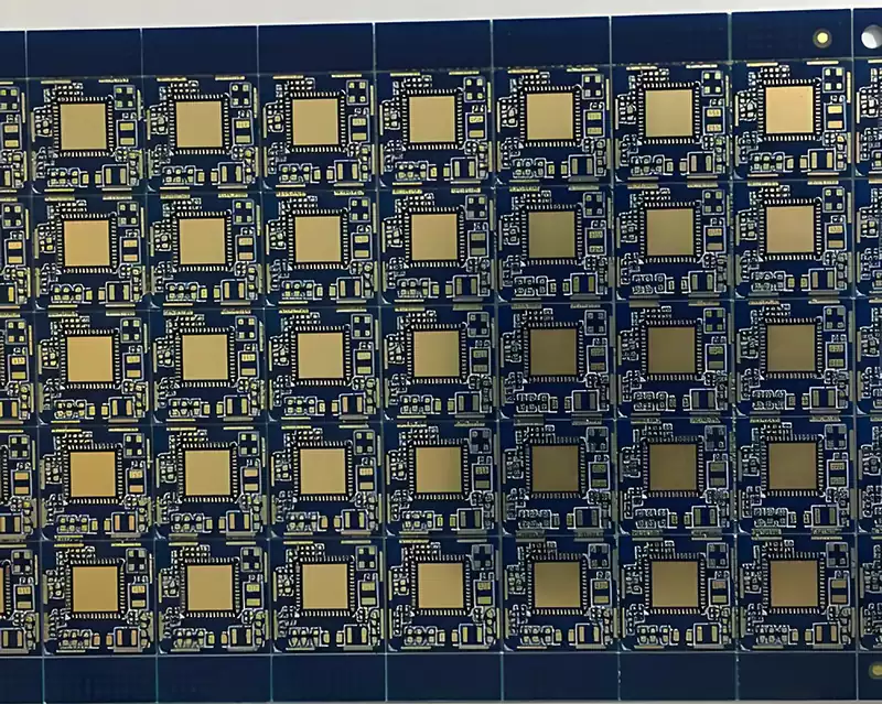
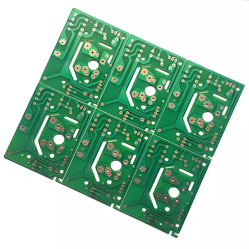
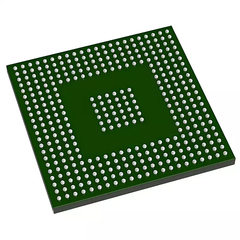
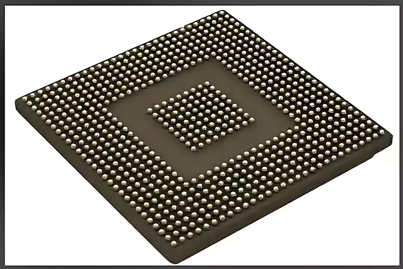
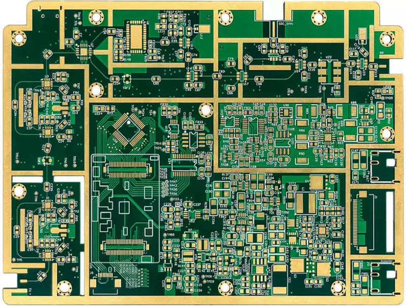
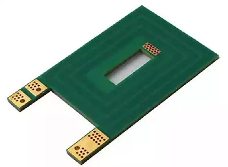
Technology Blog

Understanding PCB Socket Pins and Their Role in Reliable Electronic Connections

Understanding PCB Socket Pins and Their Role in Reliable Electronic Connections

The Fundamental Role of PCB Socket Pins in Electronic Connections In the design and assembly of electronic circuits, PCB socket pins are a crucial component for achieving electrical connections. They are typically used to establish reliable electrical interfaces between printed circuit boards (PCBs) and external modules, chips, or pluggable components. Compared to direct soldering connections, […]

copper thickness pcb

Comparison of 1oz and 2oz Copper Thicknesses and Their Role in PCB Design

In PCB design, 1oz (ounce) and 2oz are common units for measuring copper foil thickness, with 1oz approximately equating to 35 micrometres (μm). The selection of copper thickness is not arbitrary; it directly impacts the circuit board’s current-carrying capacity, thermal dissipation performance, manufacturing costs, and suitability for specific applications. It stands as one of the

FR-4 material

Limitations and Breakthrough Directions for FR-4 Materials in High-Frequency Applications?

In our PCB development work, we often face the same challenge. Engineers want higher frequency performance, but many existing boards still rely on standard FR-4 materials. On our production floor, we frequently see design teams struggle when signals begin to degrade at higher frequencies. The problem becomes clear during testing: signal loss rises, stability drops,

hdi circuit board

Electroplating Copper via Filling Technology for HDI Circuit Boards

In the evolution of HDI circuit boards towards higher density, micro-blind via filling has emerged as a core manufacturing challenge. Electroplated copper via filling technology resolves the quality and reliability issues inherent in traditional processes by converting micro-vias into solid copper pillars, thereby establishing low-loss conductive pathways. This provides critical support for high-density interconnections in

fpc antenna

FPC Antenna Laminate Design

The laminate design of FPC antennas is fundamentally an engineering solution aimed at ensuring effective signal transmission. It comprises multiple layers of materials with distinct functions, each requiring a delicate balance of electrical performance, mechanical strength, manufacturing feasibility, and cost control. Design rationale and key process parameters for each functional layerSurface protective layerServing as the

FPC

FPC Dielectric Loss Challenges and Solutions in High Frequency

With the widespread adoption of 5G communications and IoT technologies, electronic devices are rapidly evolving toward higher frequency operation, placing greater demands on the dielectric properties of FPC materials. In high-frequency signal transmission, dielectric loss has become a critical bottleneck affecting signal integrity—excessive loss can lead to signal attenuation, increased heating, and even device instability.

Dielectric Constant and Capacitance: Key Factors in High-Speed PCB Design

Dielectric Constant and Capacitance: Key Factors in High-Speed PCB Design

The Fundamental Relationship Between Dielectric Constant and Capacitance in PCB Design In electronic circuit design, the relationship between dielectric constant and capacitance is one of the fundamental concepts for understanding signal transmission and circuit stability. For PCB engineers, these two parameters not only affect the electrical characteristics of the circuit but also directly relate to

FPC antenna

FPC Antennas Principles and Manufacturing Processes

FPC antennas, formally known as flexible printed circuit antennas, are specialised antennas that integrate key functional components such as the antenna radiation unit and feed structure onto a flexible PCB substrate. The FPC antenna comprises key components including a flexible substrate, radiating elements, feed points, ground planes, and coaxial cables. The flexible substrate serves as

flexible antenna

Assembly Challenges of Flexible Antennas

The fundamental challenge in assembling flexible antennas lies in the contradiction between “physical flexibility” and “assembly precision.” The substrate is extremely thin—almost paper-like—yet it must support micron-level alignment accuracy. The circuitry is delicate and flexible, yet it must maintain signal integrity across various operating conditions. Drawing on hands-on experience from the PCB manufacturing industry, we

fpc antenna

Core Analysis of FPC Antennas

As electronic devices continue to evolve toward thinner profiles, higher frequencies, and greater functionality, antenna design faces a critical challenge: extreme space constraints without compromising performance. FPC antennas have emerged as a key solution to this problem. By combining the precision manufacturing processes of PCB technology with flexible substrates, FPC antennas represent more than just

FR4 pcb

Selection of FR4 PCB Materials for Different Layer Counts

In printed circuit board (PCB) material selection, FR4 is one of the most widely used substrates. However, even within the FR4 category, single-sided, double-sided, and multilayer structures differ significantly in performance, cost, and application scenarios. Single Sided FR4The core structure of a single-sided FR4 PCB can be summarized as “single copper layer + FR4 substrate.”Only

FR4

Selection of FR4 Material for High Voltage Circuits

In high-voltage PCB design, the insulation performance of FR4 materials directly affects the safety and stability of circuits. Among the relevant parameters, tracking resistance indicators are an important reference for evaluating insulation reliability. However, many engineers tend to confuse the tracking index with the Comparative Tracking Index (CTI) when selecting materials. Therefore, it is important

radar pcb

Differences in Frequency Bands for Automotive Radar PCB Antenna Design

All design differences between 24 GHz and 77 GHz automotive radar PCB antenna boards fundamentally stem from the distinct physical characteristics of the frequency bands themselves. Frequency determines wavelength, and wavelength directly affects antenna size, signal loss, and radiation efficiency—thereby driving adjustments across every stage of PCB design. The wavelength at 24 GHz is approximately

pcb antenna

The Critical Role and Design Considerations of PCB Antenna Ground Planes

In wireless communications, antennas are of paramount importance, and the PCB antenna ground plane, as a critical component, influences multiple aspects of antenna performance. In wireless communications, pcb antennas are of paramount importance, and the PCB antenna ground plane, as a critical component, influences multiple aspects of antenna performance. The fundamental operation of an pcb

serpentine antenna

Application of Serpentine Antennas in Small Wearable Devices

Inside products such as smart bands, TWS earbuds, smartwatches, and health monitoring patches, there is a constant tension between extremely limited internal space and ever-increasing communication requirements. Serpentine antennas, with their compact layout, high level of integration, and stable RF performance, have become a mainstream solution to this challenge, enabling a more efficient integration of

antenna pcb

Key Considerations for EMC Design of Antenna PCB

In antenna PCB design, electromagnetic compatibility (EMC) is a key factor in ensuring stable device performance and minimizing interference. As core elements of EMC design, layout and routing are not only cost-effective but also provide the most direct and efficient means of improving EMC performance. Unlike conventional PCB routing, antenna PCB routing must balance antenna

Four layer flexible circuit board

What is a four layer flexible board? FPC flexible boards can be used to manufacture four layer boards, but compared to double-layer or multi-layer FPC flexible boards, the manufacturing process is more complex and requires consideration of insulation performance, signal transmission, manufacturing process, and application areas. The four layer FPC flexible board has the advantages

antenna pcb

Selection of Rogers and FR-4 Substrates for Antenna pcb

FR-4 and Rogers, as the two most prevalent substrate materials in the antenna PCB sector, possess no inherent superiority or inferiority; their suitability depends solely on the application context. Selecting the appropriate substrate not only enables the full realisation of antenna performance but also achieves an optimal balance between cost and reliability during mass production.

high frequency antenna

Optimisation of the Solder Mask Layer for High Frequency Antennas

A high frequency antenna operates in the 300 MHz–300 GHz RF spectrum (corresponding to electromagnetic wavelengths of 1 m–1 mm). It is the core RF component responsible for bidirectional energy conversion between guided high-frequency electrical signals and free-space electromagnetic waves. High-frequency antennas serve as the transmission and reception “gateway” in wireless communication, radar, positioning, and

PCB antennas

Cost and Performance Comparison of PCB Antennas versus Ceramic Antennas

PCB antennas are directly formed by etching metal traces on the PCB substrate to create radiation units, utilizing the rigid material of the PCB for signal transmission and reception, without the need for additional antenna components. Essentially, they are a part of the PCB itself. Their structure is highly flexible, and they can be designed

fr4 substrate

Controlling Drilling Damage in FR4 Substrates to Enhance PCB Quality

Mechanical drilling constitutes the core process for achieving interlayer electrical interconnections in PCBs, yet it remains the stage where FR4 substrates are most susceptible to microscopic damage. Under the combined effects of high-speed cutting, frictional heat generation, and mechanical tearing, irreversible alterations occur in the resin and glass fibre structure of the hole walls. This

Why FR4 Plate Keyboards Are Gaining Popularity in Custom Mechanical Designs

Why FR4 Plate Keyboards Are Gaining Popularity in Custom Mechanical Designs

The Role of FR4 Plate Keyboard in Mechanical Keyboard Structure In the structural design of mechanical keyboards, the plate (positioning plate) is a crucial intermediate layer connecting the switches to the PCB. Its material selection directly impacts the overall feel, sound characteristics, and structural stability of the keyboard. In recent years, FR4 plate keyboards have

ceramic substrate

Differences and Selection Between Aluminide and Alumina Ceramic Substrates

Ceramic substrates, as critically important materials within PCBs, play a pivotal role in enhancing PCB performance through their unique physical and chemical properties. Among these, aluminium oxide (Al₂O₃) and aluminium nitride (AlN) are the two most commonly used ceramic substrates. While they share a similar appearance and overlapping applications, they exhibit significant differences in core

4 layer pcb

4 layer PCB Layering Techniques for Achieving Extremely Low Noise Routing

As one of the most widely adopted specifications in the industry, the cost-effectiveness and practicality of 4 layer PCBs are beyond question. However, achieving low noise floor hinges not on increasing layer count, but on meticulous control of stack-up logic, ground plane integrity, signal partitioning, and return paths. This article, grounded in practical PCB manufacturing

Scroll to Top