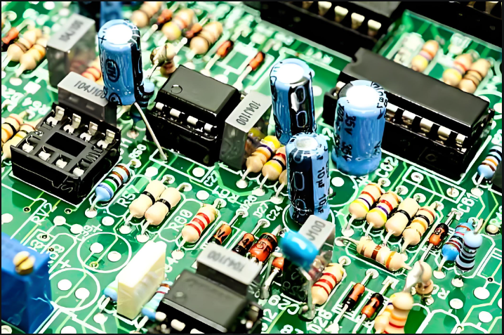
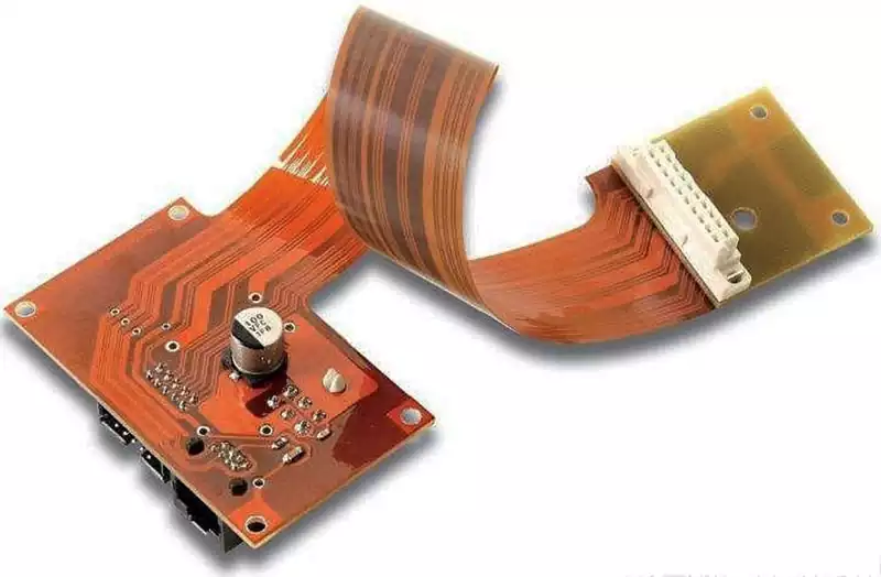
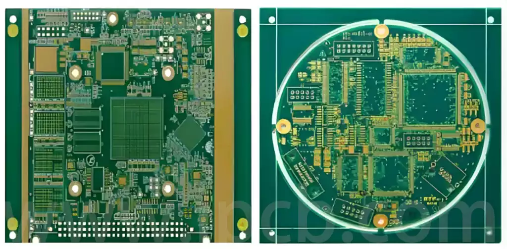
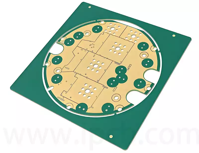
After the PCB circuitry is etched, a layer of ink (green ink, blue ink, black ink, etc.) needs to be applied. However, ink is liquid and has flowability. During the curing process after application, uneven ink distribution may occur, primarily around drill holes. In such cases, certain areas may appear under a magnifying glass to have missed ink application, resembling exposed copper surfaces—this is known as pseudo pcb exposed copper.
Causes of false PCB exposed copper
- During the solder mask process, when producing end-of-line boards, a plugging mesh was not used for production. Instead, an empty mesh was used for continuous printing with plugging, resulting in incomplete plugging. After baking, the ink contracted, causing false copper exposure at the edges of the holes.
- During the rework of solder mask removal, ink inside the holes was not thoroughly cleaned, causing the ink to fail to fully fill the holes during the second printing process, resulting in incomplete hole filling and pseudo pcb exposed copper.
- Currently, during the printing and hole-filling process, the first side is directly placed on the printing machine table. Due to the flat surface of the table, air cannot be effectively expelled from the holes, leading to incomplete filling of some holes and causing pseudo-copper exposure.
Hazards of PCB exposed copper
- Impact on signal transmission: The circuit board is a critical component of electronic products, with conductive traces often being extremely small.PCB exposed copper can reduce the distance between conductive traces and the insulating layer, thereby affecting the stability and reliability of signal transmission.
- Reduced conductivity: PCB exposed copper can reduce the conductivity of the circuit board, thereby impacting the overall operational efficiency of the circuit.
- Increased PCB failure rate: After exposed copper, abnormal current concentration may occur on the PCB, which, over time, may increase the failure rate of the PCB.
- Increased repair and maintenance costs: If PCB exposed copper, it may require repair or replacement, thereby increasing repair and maintenance costs.
Exposed copper standards
To standardise PCB copper leakage issues, the industry has established a series of standards, primarily covering the following aspects:
- IPC-A-600H ‘Acceptability Standards for Electronic Assembly Products’: This is one of the internationally recognised IPC standards, with Section 3 ‘Special Requirements for Board Surfaces’ detailing the standard requirements for PCB exposed copper;
- J-STD-001 ‘Standard Requirements for Electronic Assembly Processes’: This standard, issued by the American Electronics Association (IPC), provides detailed specifications for PCB board soldering processes and regulates copper leakage issues on PCB boards;
- Customer Requirements: Different electronic product manufacturers may impose additional requirements on copper leakage issues on PCB boards based on their specific needs, and suppliers must comply with these requirements as appropriate.
Solutions for addressing false PCB exposed copper
- Adjust the squeegee pressure based on the type of screen, ink characteristics, and PCB requirements. Reasonably adjust the squeegee pressure. By testing different pressure values and observing the ink application on the PCB, you can determine the optimal pressure that ensures adequate ink transfer without damaging the screen. For example, conduct a pressure test before printing, gradually increasing the pressure until the ink is evenly transferred.
- Control printing speed Determine an appropriate printing speed by considering factors such as ink drying speed and stencil aperture rate. Ensure production efficiency while avoiding insufficient ink transfer due to excessive speed. Conduct multiple trials to observe ink application effects at different speeds and determine the optimal printing speed.
- Adjust the squeegee depth and angle. Properly set the contact depth and angle between the squeegee and the screen. Typically, the squeegee depth should be adjusted based on the screen thickness and ink characteristics to ensure effective ink transfer through the screen openings onto the PCB. Additionally, select an appropriate squeegee angle based on experience and test results, generally between 45–60 degrees, to ensure uniform ink application.
- Ensure sufficient blade length Select a blade of appropriate length to ensure it fully covers the screen width during printing. When installing the blade, check that it is installed flat to avoid uneven ink distribution in certain areas due to insufficient blade length.
- Adjust the ink concentration Adjust the ink concentration appropriately according to printing requirements. If the ink concentration is too high, add an appropriate amount of diluent to reduce the concentration and improve ink flowability, enabling it to pass through the screen mesh holes more effectively. After adjusting the ink concentration, conduct a test print to observe the ink application effect on the PCB board.
- Optimise screen spacing. Set the spacing between the screen and the PCB board reasonably based on the flatness of the screen and PCB board, as well as the characteristics of the ink. This is typically achieved by adjusting the screen mounting mechanism of the printing machine. Smaller spacing facilitates ink transfer, but care must be taken to avoid damage caused by contact between the screen and PCB board. A spacing of 0.5–2 millimetres is generally appropriate.
PCB exposed copper is a common issue in production, typically resulting from improper solder mask processes or via handling. Although it may not always affect functionality, it still requires precise adjustment of printing parameters and continuous optimisation of production processes to ensure the long-term reliability and quality of the PCB.
