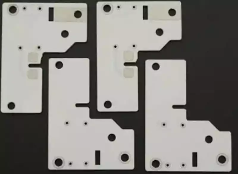
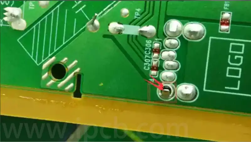
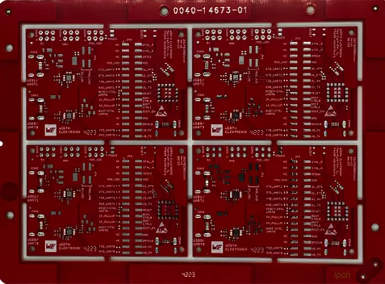
Reflow soldering of ceramic circuit boards constitutes a critical process in achieving component encapsulation, wherein the precision of temperature curve control serves as the very lifeline determining soldering quality. Ceramic materials inherently possess high hardness yet significant brittleness, coupled with a thermal expansion coefficient markedly different from metallic solders.
Should the temperature curve be improperly designed, consequences range from minor issues such as cold solder joints and poor solder wettability to severe outcomes including substrate cracking and component damage, directly compromising product reliability and service life. Even with identical ceramic substrates and identical solder compositions, a precise temperature profile can maximise soldering yield. Conversely, an inadequate profile may negate the performance advantages of high-quality materials. How, then, should the temperature profile for ceramic circuit board reflow soldering be scientifically designed and rigorously controlled?
Special Challenges Posed by Ceramic Properties to Reflow Soldering
The fundamental difference between reflow soldering ceramic circuit boards and traditional FR-4 circuit boards lies in the unique physical properties of ceramic materials. Common ceramic substrates (such as aluminium oxide, aluminium nitride, and LTCC low-temperature co-fired ceramics) exhibit a coefficient of thermal expansion (CTE) of merely 4-7 ppm/°C, significantly lower than that of tin-lead solder (18-22 ppm/°C) and lead-free solder (20-24 ppm/°C). Concurrently, ceramics exhibit excellent thermal conductivity yet possess extreme brittleness and poor thermal shock resistance. These properties impose critical requirements on the temperature profile: gradual heating, sufficient dwell time, precise peak temperature control, and controlled cooling to prevent thermal stress from abrupt temperature changes or excessive differentials.
The primary challenge lies in thermal expansion coefficient mismatch. During soldering, ceramic substrates, solder, and component leads undergo synchronous temperature changes yet exhibit markedly different expansion rates. Excessively rapid heating or cooling generates substantial thermal stresses, causing micro-cracks or outright fracture in the substrate. Ceramics’ low thermal shock resistance further amplifies the hazards of temperature fluctuations. When the rate of temperature change exceeds the ceramic’s tolerance limit (typically ≤5℃/s), internal structural damage occurs even without visible cracks, reducing product lifespan. Additionally, ceramics’ high thermal conductivity accelerates heat transfer; excessive temperature differentials across the profile can cause localised over-soldering or insufficient soldering.
Precise Four-Stage Control of Ceramic Circuit Board Reflow Temperature Profiles
Standard reflow profiles comprise four stages: preheating, soak, reflow, and cooling. Tailored to ceramic circuit board characteristics, each stage requires precisely calibrated temperature parameters and timing to establish the core logic of ‘gradual heating – thorough soaking – precise peak – gradual cooling’.
1.Preheating Stage: Gentle Temperature Rise to Avoid Thermal Shock
The core objective of the preheating stage is to gradually elevate the ceramic PCB’s temperature, removing moisture and flux volatiles from the solder paste while preventing thermal stress caused by abrupt temperature increases. The preheating rate for ceramic circuit boards must be strictly controlled, typically set at 1–3°C/s—significantly lower than the 3–5°C/s used for conventional FR-4 boards. Excessive heating rates create substantial temperature differentials between the surface and interior of the ceramic substrate. Combined with thermal expansion differences between the substrate and solder, this readily induces transient thermal stresses that may cause cracking.
The preheating temperature endpoint must be controlled between 150-180°C, with specific values adjusted according to solder paste type—lead-free paste typically requires an endpoint near 180°C, while lead-tin paste may be set slightly lower at 150-160°C. The preheating duration is recommended to be set at 60–120 seconds, ensuring uniform temperature distribution across the entire circuit board and allowing sufficient volatilisation of the solder paste. This prevents subsequent stages where rapid expansion of volatiles causes solder splatter and void formation. Note that temperature uniformity deviation during preheating should be controlled within ±5°C. This can be achieved by adjusting the hot air circulation rate of the reflow oven to prevent excessive localised heating.
2.Holding Phase: Ensuring Full Wetting and Solder Paste Activation
The holding phase (also termed the stabilisation phase) serves as the critical transition between preheating and reflow. Its primary function is to maintain stable temperatures for the ceramic circuit board and components, ensuring full flux activation while enabling initial wetting of the ceramic circuit board and component leads by the solder paste. For ceramic circuit boards, the holding temperature should be set between 170–190°C (lead-free paste) or 140–160°C (lead-containing paste), with a holding duration of 60–90 seconds.
Adequate temperature stabilisation enables the flux to perform optimally—removing oxidation layers from ceramic pad surfaces and component leads, reducing solder surface tension, and laying the groundwork for solder spreading during subsequent reflow. Insufficient stabilisation time results in inadequate flux activation, leading to poor solder wetting and cold solder joints. Conversely, excessive dwell time may deplete the flux, potentially compromising its protective function and allowing pad re-oxidation. Furthermore, temperature stability must be maintained throughout the dwell phase to prevent fluctuations, as these disrupt the flux activation rhythm and adversely affect soldering quality.
3.Reflow Stage: Precise Temperature Control to Regulate Solder Fusion Rhythm
The reflow stage constitutes the pivotal phase where solder transitions from solid to liquid state, with the accuracy of the temperature profile directly determining soldering quality. For ceramic circuit boards, critical control parameters during reflow include heating rate, peak temperature, and peak dwell time to prevent substrate and component damage from excessive heat.
The heating rate from isothermal to peak temperature should be maintained at 2–3°C/s to prevent thermal stress accumulation. Setting the peak temperature is critical and must be determined comprehensively based on the solder paste melting point and the ceramic substrate’s heat resistance: – For lead-free solder paste (e.g., SAC305, melting point 217°C), the peak temperature is recommended at 240-250°C. – For lead-tin solder paste (melting point 183°C), the peak temperature is recommended at 210-220°C. Note that peak temperatures must not exceed the ceramic substrate’s thermal endurance limit. Aluminium oxide ceramics exhibit long-term thermal resistance exceeding 1600°C, allowing unproblematic short-term peak reflow temperatures. However, LTCC ceramics possess lower thermal tolerance; peak temperatures must be maintained below 250°C to prevent damage to internal wiring and packaging structures.
The peak dwell time (i.e., duration at peak temperature) must be strictly controlled between 10–30 seconds. Insufficient dwell time prevents adequate solder fusion and spreading, leading to issues such as insufficient solder volume and incomplete solder joints. Excessive dwell time accelerates interfacial reactions between the ceramic circuit board and solder at high temperatures, forming excessively thick intermetallic compounds that degrade joint mechanical properties and may cause component overheating damage.
4.Cooling Phase: Gradual Temperature Reduction to Minimise Thermal Stress Damage
The cooling phase involves the transition of solder from liquid to solid state. Its core requirement is gradual temperature reduction to mitigate thermal stress arising from differing thermal expansion rates between the ceramic substrate, solder, and components. The cooling rate for ceramic circuit boards must be strictly controlled at 1–2°C/s, significantly lower than the 3–5°C/s typical for conventional FR-4 boards.
Gradual cooling synchronises temperature reduction between the ceramic circuit board and solder joints, preventing premature solidification of solder while the substrate continues to contract. This avoids excessive tensile stress on joints, which could cause solder joint cracking or substrate fracture. The recommended final cooling temperature should be below 100°C, at which point the solder is fully solidified and the circuit board may be removed. It is important to note that direct cold airflow should be avoided during cooling. Natural cooling or gentle hot-air cooling methods are preferable to prevent localised temperature drops that could induce thermal stress. Furthermore, the cooled circuit board must be left to rest for a period to allow the temperature to stabilise uniformly, thereby avoiding stress release during subsequent handling due to residual thermal effects.

Temperature Curve Adaptation for Different Ceramic Circuit Board
Variations in heat resistance and thermal expansion coefficients among ceramic circuit boards necessitate tailored reflow soldering temperature curves to achieve optimal results.
Alumina Ceramics (Al₂O₃): As the most commonly used ceramic circuit board, alumina ceramics offer excellent heat resistance and high mechanical strength. Standard parameters may be employed: peak temperature for lead-free solder paste at 240–250°C, peak dwell time of 20–30 seconds, and cooling rate of 1–2°C/s. Note that high-purity alumina ceramics (e.g., 99.6% alumina) exhibit slightly higher brittleness than lower-purity variants. Heating and cooling rates may be appropriately reduced to 1–2°C/s.
Aluminium Nitride Ceramics (AlN):
AlN ceramics possess significantly superior thermal conductivity to alumina but exhibit greater brittleness and slightly weaker thermal shock resistance. The temperature profile requires further optimisation: – Control the heating rate at 1-2℃/s, extending the isothermal period to 80-90 seconds to ensure uniform temperature distribution. – Maintain the peak temperature at 240-245℃, reducing the peak dwell time to 10-20 seconds to avoid prolonged exposure to high temperatures. – Strictly control the cooling rate below 1℃/s to minimise thermal stress damage.
LTCC (Low-Temperature Co-fired Ceramics): Containing metallic interconnects and glass phases, LTCC ceramics exhibit lower heat resistance. Peak temperature must be strictly controlled below 240°C, ideally between 235-240°C. Both heating and cooling rates should be maintained at 1-2°C/s, with a holding time of 60-80 seconds. The peak dwell time should be reduced to 10-15 seconds to prevent softening and deformation of the glass phase, which could cause internal wiring displacement.
Common Issues and Solutions in Temperature Profile Control
In actual production, multiple problems frequently arise during temperature profile control for reflow soldering of ceramic circuit boards. Targeted troubleshooting and optimisation are essential to enhance soldering yield.
Issue 1: Substrate Cracking
Primarily caused by excessive thermal stress accumulation due to overly rapid heating or cooling rates, or excessively high peak temperatures. Solution: Reduce heating and cooling rates to 1-2°C/s; strictly control peak temperatures to avoid exceeding the ceramic substrate’s heat resistance limit; inspect the reflow oven’s temperature uniformity, repair faulty heating zones, and ensure synchronised temperature changes across all PCB areas.
Issue 2: Cold solder joints and poor solder wetting. Primarily caused by insufficient dwell time, inadequate flux activation, or excessively low peak temperatures coupled with short dwell periods. Solution: Extend dwell time to 80-90 seconds to ensure complete flux activation; moderately increase peak temperature (without exceeding thermal tolerance limits) and prolong peak dwell time to 20-30 seconds to guarantee thorough solder fusion and spreading; verify solder paste freshness and replace with active paste if expired.
Issue 3: Solder joint voids. Primarily caused by insufficient preheating temperature or duration, preventing adequate volatilisation of flux components. Solution: Increase preheat endpoint temperature to 170–180°C and extend preheat time to 100–120 seconds; optimise temperature profile during the constant temperature phase to ensure complete volatilisation; verify solder paste moisture content and avoid using dampened paste.
Issue 4: Component damage. Primarily caused by excessively high peak temperatures or prolonged peak dwell times. Solution: Reduce peak temperature by 5–10°C and shorten peak dwell time to 10–20 seconds; for thermally sensitive components, implement localised cooling measures or select components with higher heat resistance; optimise the temperature profile to avoid prolonged exposure to high-temperature zones.
Controlling the temperature profile for reflow soldering of ceramic circuit boards constitutes a systematic engineering endeavour that balances material properties, soldering principles, and production realities. From the gradual heating during preheating, through thorough activation during the constant-temperature phase, to precise temperature control during reflow, and finally the gradual cooling during the cooling phase – parameter settings for each stage must be tailored to ceramic characteristics. This prevents thermal stress damage and ensures soldering reliability.


