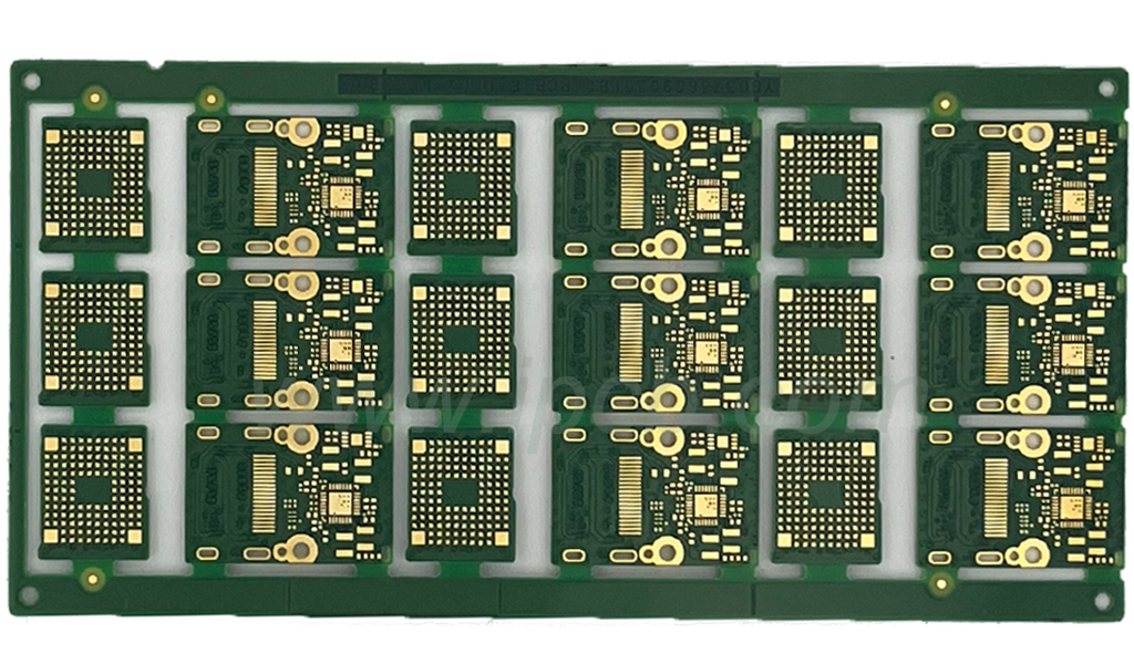
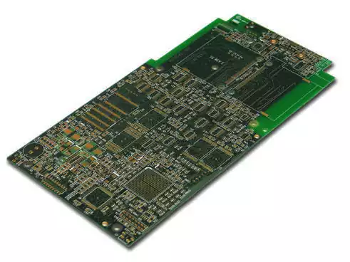
High-layer printed circuit boards typically refer to boards exceeding four layers. Compared to traditional double-layer boards, they enable more complex circuit designs by embedding multiple conductive layers internally. For instance, an eight-layer board may comprise four signal layers, two power layers, and two ground layers. These layers are separated by insulating materials (such as prepreg) and interconnected vertically via vias. This architecture substantially increases circuit density while effectively mitigating signal interference, thereby meeting the demands of high-speed data transmission.
Structural Characteristics of High-Multilayer Circuit Boards
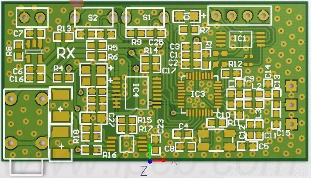
- Multilayer Structure: High-multilayer printed circuit boards comprise multiple conductive layers and insulating layers, with each conductive layer connected via micro-vias or blind vias. This configuration offers greater design flexibility to accommodate complex electronic equipment requirements.
- High-density integration: The multilayer design enables greater component integration within limited space. This not only enhances electronic device performance but also reduces overall size and weight.
- Superior signal transmission: Precise interlayer connections between conductive layers ensure rapid and accurate signal propagation. This is critical for high-speed, high-frequency electronic equipment.
Application Domains of High-Multilayer printed circuit boards
Within the communications equipment sector, the rapid advancement of 5G technology has fuelled growing demand for high-frequency, high-speed signal transmission. High-multilayer PCBs play a pivotal role in this domain due to their unique advantages.
In computing and server systems, high-performance computers and servers must process vast data volumes and complex instructions, posing stringent challenges to PCB signal transmission rates and reliability. The widespread adoption of high-layer PCBs precisely meets these demanding requirements.
The medical electronics sector similarly relies heavily on high-layer printed circuit boards. Their reliability and signal precision are critical for medical equipment, making high-layer PCBs essential components for ensuring the efficient and stable operation of such devices.
Furthermore, the aerospace and military sectors impose stringent requirements on equipment performance, reliability, and interference resistance. High-layer PCBs, with their outstanding electrical properties and design flexibility, play an indispensable role in these fields.
Why choose high-layer printed circuit boards?
Compared to single-layer or double-layer boards, high-layer boards offer the following advantages:
- High integration: Accommodates more traces per unit area, reducing equipment size;
- Strong interference resistance: Dedicated power and ground planes minimise electromagnetic interference (EMI);
- Superior thermal management: Multi-layer structure facilitates heat dissipation channel design, enhancing device stability;
- Design flexibility: Enables more complex circuit layouts through blind and buried via techniques.
Compared to conventional printed circuit boards products, high-layer boards feature greater thickness, increased layer count, denser traces and vias, larger unit dimensions, and thinner dielectric layers. This necessitates stricter requirements for inner layer space, layer-to-layer alignment, impedance control, and reliability.
Manufacturing Challenges for High-Multilayer printed circuit boards
Interlayer Alignment Difficulties
Given the substantial number of layers in high-layer boards, clients increasingly demand stringent alignment tolerances during the design phase, typically setting interlayer alignment tolerances at ±75μm. However, factors such as the typically larger unit dimensions in high-layer board designs, variations in temperature and humidity within the pattern transfer workshop environment, the cumulative misalignment caused by inconsistent expansion and contraction between different core board layers, and the impact of interlayer positioning methods, collectively increase the difficulty of controlling interlayer alignment in high-layer boards.
Challenges in Inner Layer Fabrication
High-layer boards employ specialised materials such as high TG, high-speed, high-frequency, thick copper, and thin dielectric layers, imposing higher standards for inner layer fabrication and pattern dimension control. For instance, ensuring impedance signal transmission integrity significantly elevates the complexity of inner layer production. Specifically:
- Small line widths and spacing frequently result in open/short faults and micro-shorts, leading to lower product yield rates; The greater number of signal layers in densely packed circuits increases the probability of missed defects during inner layer AOI (Automated Optical Inspection). The relatively thin core thickness of inner layers makes them prone to wrinkling during fabrication, leading to exposure defects, and curling during the etching process. Furthermore, as high-layer boards are predominantly system boards with larger unit dimensions, the cost of scrap in finished products is comparatively high.
Laminating Challenges
During lamination, stacking multiple inner core boards with prepreg sheets frequently leads to defects such as board slippage, delamination, resin voids, and trapped air bubbles. Consequently, stackup design must comprehensively evaluate material thermal resistance, voltage tolerance, resin fill volume, and dielectric thickness to establish scientifically sound lamination protocols for high-layer boards.
Owing to the substantial number of layers in high-layer printed circuit boards, maintaining consistent dimensional expansion/contraction control and dimensional coefficient compensation proves challenging in actual production. Concurrently, the thinness of interlayer insulation layers frequently results in failure to pass interlayer reliability testing.
Drilling Challenges
The use of specialised boards featuring high TG, high-speed, high-frequency, and thick copper layers increases the difficulty in achieving smooth drill roughness, minimising burrs, and removing drill residue. The cumulative total copper thickness and board thickness across multiple layers predispose drill bits to breakage. Dense BGA placements and narrow hole wall spacing contribute to CAF failures. Board thickness also facilitates the occurrence of skewed drilling.
High-layer printed circuit boards offer significant advantages and widespread applications, yet their manufacturing presents formidable challenges. Nevertheless, technological advancement continues unabated. Future breakthroughs in manufacturing bottlenecks are anticipated, poised to further empower the electronics industry’s development.