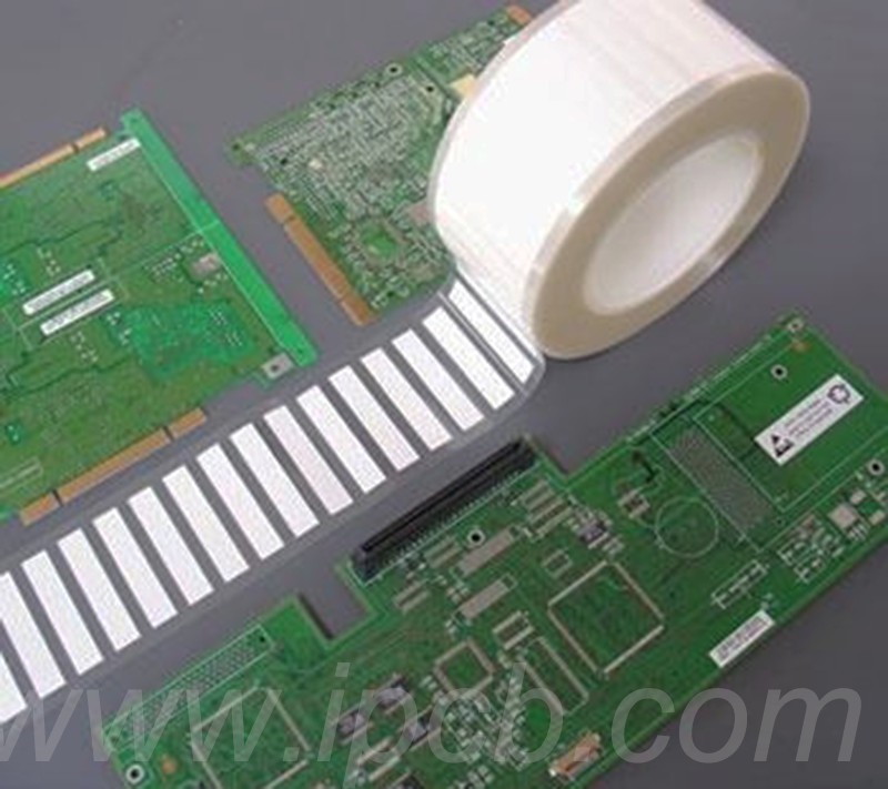
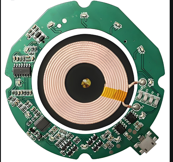
Circuit board labels are the PCB (Printed Circuit Board, Printed Circuit Board) technology based on the manufacture of high-frequency RFID tags. PCB tags can be divided into a variety of types according to power, size, frequency and other factors, according to the frequency distinction between ultra-high-frequency PCB anti-metal tags, high-frequency PCB anti-metal tags and so on. Distinguished by size there are large pcb anti-metal tags, there are also miniature pcb anti-metal labels.
Circuit board labels play a vital role in the PCB design and manufacturing process:
Stamped holes: Stamped holes are mainly used in the design of patchwork boards to facilitate the production and processing of multiple small-sized PCBs connected together to improve productivity and reduce costs. After production is complete, the individual small boards can be separated by a simple breakout or cutting operation. In addition, stamp holes in the modular design can achieve easy assembly and disassembly, while ensuring a certain degree of connection strength and electrical performance for easy product maintenance and upgrading.
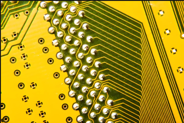
Types of vias: Vias include through holes, blind holes and buried holes, which play a key role in multilayer PCB design. Through holes run through the entire board layer to achieve electrical connections between different layers; blind holes extend only to one or several intermediate layers inside, reducing the use of through holes and improving wiring density; buried holes are located between the internal layers, and the ends do not extend to the surface layer, further improving the flexibility and density of the wiring. These designs help optimise circuit layout and reduce interference and loss in signal transmission.
Anti-solder pads: Anti-solder pads (also known as solder resist pads) prevent solder from spreading in areas where it is not needed during the soldering process, ensuring that solder forms a good solder connection only at the designated soldering points and avoiding undesirable conditions such as short circuits. In addition, it also protects the copper foil lines from oxidation and corrosion, improving the reliability and service life of the PCB.
Benchmarking: Benchmarking is a special pattern or marking used for positioning and calibration during the production and assembly of PCBs. In photolithography, drilling, placement and other processes, the datum marking helps the equipment to be accurately positioned to ensure the accuracy and consistency of the production process.
Spark Gap: Spark gaps are used for ESD (electrostatic discharge), current surge and overvoltage protection. When high voltage ionises the air between two terminals, the spark gap creates a spark between them, protecting the circuit from damage. Although the spark gap protection method has the disadvantage of changing performance over time, it is still an effective protection measure in the absence of better protection methods.

Labelled circuit boards are circuit boards that have labels or logos attached to them, and these labels are usually used to identify the function, model number, date of manufacture, and other information about the circuit board. These labels can be fixed on the circuit board by printing, attaching, etc. for easy identification and management.
Labelled circuit boards are widely used in a variety of electronic devices, mainly used in the following areas:
Marking function: The function of the circuit board is marked by the label, which is convenient for technicians to quickly identify the role of the circuit board and the connection method.
Production management: In the production process, the label can help track the circuit board manufacturing process and quality control.
Maintenance and repair: the information provided by the label helps technicians to carry out maintenance and troubleshooting of equipment.
Fabrication Process for Labelled Circuit Boards
The fabrication of labelled circuit boards usually involves the following steps:
Design:Design the board layout and label placement according to requirements.
Fabrication:The labels are attached to the board using printing or attaching techniques.
Inspection:Ensure that the labels are secure and do not affect the functionality of the board.
Material Selection for Label circuit Boards
Label material selection depends on the specific application requirements and environmental conditions.Common materials include:
High temperature resistant materials: such as PI (polyimide) materials for high temperature environments.
Corrosion-resistant materials: suitable for use in humid or corrosive environments.
High-adhesion materials: Ensure that labels stick firmly in a variety of conditions.
Through these steps and material selection, you can ensure that the circuit board with label excels in a variety of applications and meets different needs.
Circuit board labels and labelled circuit boards play a pivotal role in the manufacture of modern electronic devices. Every step of the way, from delicate PCB design to complex production processes and demanding material selection, ensures the high performance and reliability of the boards. Design elements such as stamp holes, via types, solder-proof pads,datum marks and spark gaps not only optimise the circuit layout, but also enhance signal transmission efficiency and electrical performance.The labelled circuit boards,on the other hand, greatly facilitate the identification and management of electronic devices through identification functions, production management, maintenance and repair.


