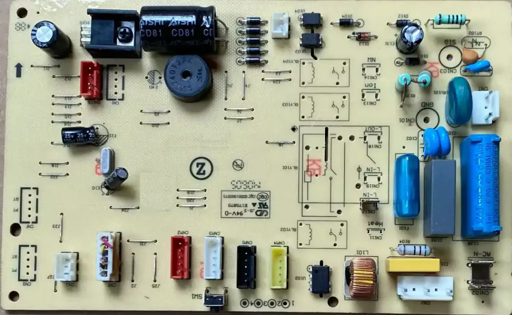
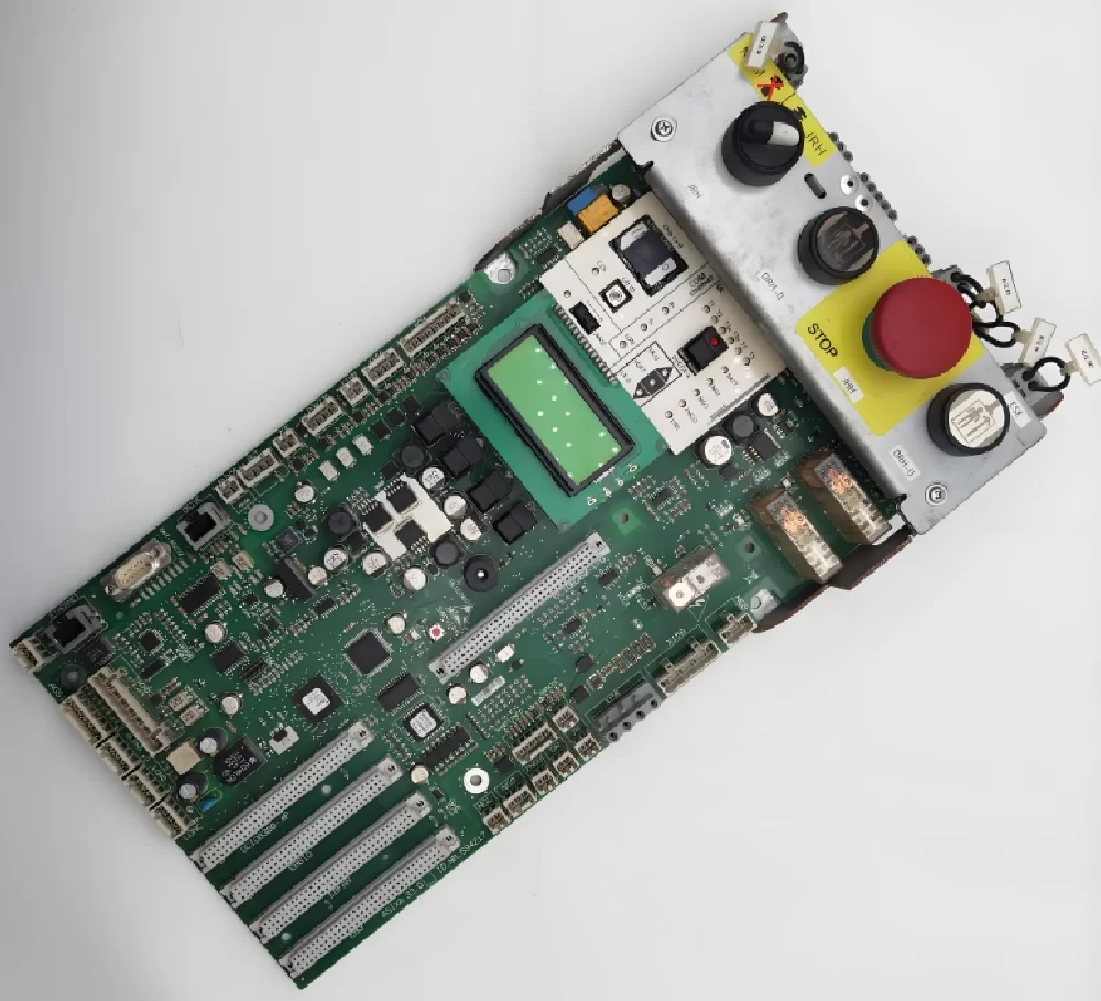
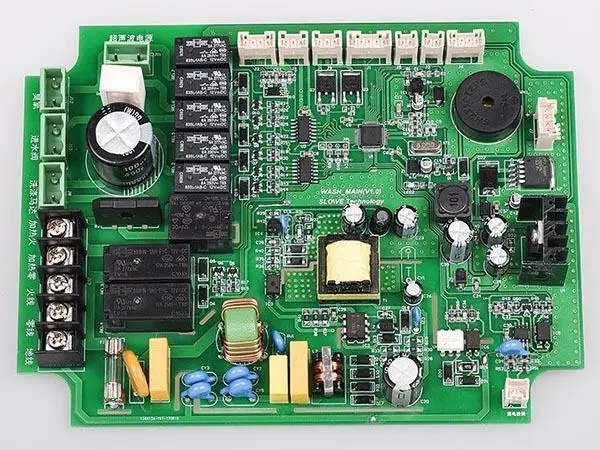
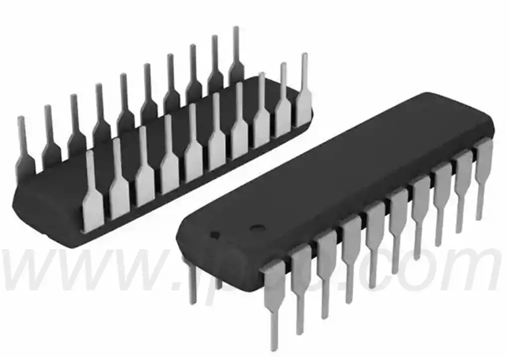
DIP package assembly, also known as Dual In-line Package (DIP), is an assembly method that requires the pins of an electronic component to be inserted into a through-hole of a printed circuit board (PCB), and then secured using soldering techniques such as wave soldering. The DIP package process is particularly suitable for larger electronic components with a large number of pins, such as high-power components, high-frequency components, and components that need to operate in high-temperature environments. Given that these components are usually operated under more severe operating conditions, they are not suitable for assembly using surface mount technology (SMT). The DIP packaging process ensures that these special components are reliably connected by directly inserting the pins into the PCB holes and soldering them in place.
Dual In-line Package plug-in has a simple packaging process, easy soldering operations, easy insertion and removal, as well as cost-effective multiple advantages. However, DIP plug-ins are not perfect, its shortcomings are also significant. For example, DIP plug-in component pins in the insertion and removal operations are very susceptible to damage, which directly leads to component reuse and reliability of the decline. Especially in applications that require frequent plugging and unplugging, the service life of DIP insert assemblies can be significantly reduced. In addition, the package size and thickness of DIP insert components are relatively large, which undoubtedly constitutes an obstacle to the realisation of high-density integration.
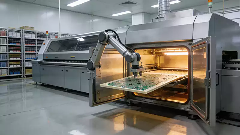
Compared to Dual In-line Package plug-ins, SMT mounting technology, i.e. Surface Mounted Technology (Surface Mounted Technology), exhibits very different characteristics. The technology uses automated equipment to accurately fit small, miniature electronic components to the surface of the circuit board and fix them through soldering, making SMT the preferred choice for large-scale, batch electronics manufacturing due to its high-density integration, high production efficiency, and high reliability.
Advantages of SMT placement technology:
① High efficiency: SMT placement process can greatly improve the speed of product assembly, so that the entire placement process can be completed quickly.
② High accuracy: This processing technology can achieve higher uniformity and accuracy in a more compact package.
Miniaturisation and lightweighting: SMT SMD uses smaller component packages, which helps to optimise the use of circuit board space.
Durability: SMT SMD components show excellent resistance to vibration and shock, thus ensuring a longer service life.
⑤ High flexibility: SMT SMD technology enables easy and quick replacement of components, providing great convenience for subsequent maintenance work.
⑥ Material cost saving: This process helps to reduce the use of materials, which in turn reduces the overall cost.
However, SMT technology also faces some limitations. For example, when dealing with components that are large in size and have a high number of pins, SMT placement may not be able to meet the requirements of high-density placement. In addition, SMT SMD processing sets high standards for the design and manufacture of PCB boards, which must ensure the accuracy and flatness of the pads to prevent defects from occurring during the soldering process.
The application areas of DIP and SMT technologies:
DIP technology is more inclined to specific application scenarios that deal with high mechanical stress environments and stringent heat dissipation requirements, while SMT technology dominates in the pursuit of high-efficiency, low-cost and high-density electronics manufacturing. In practice, it is critical to select the most appropriate packaging technology based on product uniqueness and specific needs.
DIP technology is often used for electronic components that require strong mechanical stress or excellent heat dissipation. The pins are soldered directly through the holes of the PCB (Printed Circuit Board), creating both a robust mechanical connection and a reliable electrical connection. This package design allows DIP components to withstand higher mechanical stress, so in areas such as military, aerospace and other high-reliability requirements, DIP technology still maintains a certain application space. In addition, for larger power, significant heat generation components, DIP packaging can provide more excellent heat dissipation.
SMT technology is widely used in consumer electronics, communications equipment, computers and many other fields. Given the small size and light weight of SMT components, help promote the miniaturisation of electronic products, lightweight process.At the same time,SMT technology by virtue of automated equipment, accurate placement and efficient welding,greatly improving production efficiency,and effectively reduce production costs. Therefore, SMT technology shows significant advantages in the application scenarios that require large-scale mass production and the pursuit of high efficiency and low cost. In addition, SMT technology is also particularly suitable for high-density,high-precision electronic assembly operations, such as mobile phones, tablet PCs and other consumer electronics products in the motherboard manufacturing process.
Cost comparison between DIP and SMT:
From the perspective of equipment acquisition, SMT technology tends to require a larger capital investment because it relies heavily on automated devices to achieve high-speed and accurate placement and soldering operations. In contrast, DIP technology is less expensive because it relies more on manual or semi-automated equipment to complete the insertion and soldering process.
When looking at productivity, the advantages of SMT technology are obvious. With its automated devices and precision placement technology, SMT can achieve high-speed and efficient production rhythm,a placement machine per hour can easily mount hundreds or even thousands of components, perfectly suited to the actual needs of mass production. In contrast, the production efficiency of DIP technology is obviously low, plug-in machine operating speed is far from being comparable with the chip machine, and welding links are relatively cumbersome, prone to welding quality problems.
In terms of labour costs, DIP technology due to low productivity and high dependence on manual operation, so labour costs are relatively high. SMT technology, although the initial purchase of equipment on the larger investment, but thanks to its excellent production efficiency and high yield, can effectively dilute the unit cost in large-scale production.
From the soldering quality point of view, SMT technology with the help of automated devices and advanced testing technology to control the quality, quality stability is higher. While DIP technology is more dependent on manual operation, soldering quality is more susceptible to human interference, which may lead to quality fluctuations and additional maintenance costs.
DIP(Dual In-line Package) and SMT as the two mainstream technologies in the field of electronic packaging, each has its own unique advantages and limitations. In practical application, we need to choose the appropriate packaging technology according to the uniqueness of the product and specific needs. With the continuous development and innovation of electronic technology, DIP and SMT technology will continue to evolve and improve.
