Introduction
With the continuous improvement of global environmental awareness, green manufacturing has become an irreversible trend in the electronics industry. Major markets such as Europe and the United States have put forward stricter environmental standards for electronic products. Among them, ROHS PCB, as a basic compliance requirement, is playing the dual role of “pass” and “quality label”. Whether it is heat dissipation, reliability, or export compliance, it is closely related to ROHS requirements.
In the past decade, ROHS (Restriction of Hazardous Substances) has gradually become one of the core standards of the electronics industry. Its core is to limit the use of ten hazardous substances such as lead, cadmium, mercury, hexavalent chromium, polybrominated biphenyls, and polybrominated diphenyl ethers to reduce the negative impact on the environment and human health. As a key carrier of electronic products, every link of PCB manufacturing materials and processes needs to respond to this regulatory requirement in order to meet the dual inspection of supervision and market.
For technicians, ROHS immediately means an upgrade of production processes: recalibration of lead-free reflow curves, replacement of harmful flame retardants, selection of solder and flux, pollution removal capacity of equipment, etc. all need to be considered in place; for procurement/foreign trade, ROHS compliance has become an important part of negotiations, and even determines import and export capabilities; for ordinary customers and newcomers in the industry, understanding ROHS is a compulsory course for entering the industry, and it also helps to judge the compliance of the supply chain.
More importantly, green manufacturing is not just about meeting regulations, but also has strategic significance. ROHS PCB compliance is an important foundation for enterprises to achieve green transformation and improve market trust and competitiveness. Manufacturers with good ROHS control capabilities often have more advantages in customer selection, more efficient and transparent supply chain management, and are also in a leading position in subsequent quality accidents and environmental risks.
Therefore, understanding ROHS PCB is not just about “learning regulations”, but also about mastering the core capabilities of future green electronic manufacturing. Next, we will go deeper, from definition to practice, from process to trend, step by step to unveil the full picture of ROHS PCB green manufacturing.
The profound impact of RoHS on the PCB industry
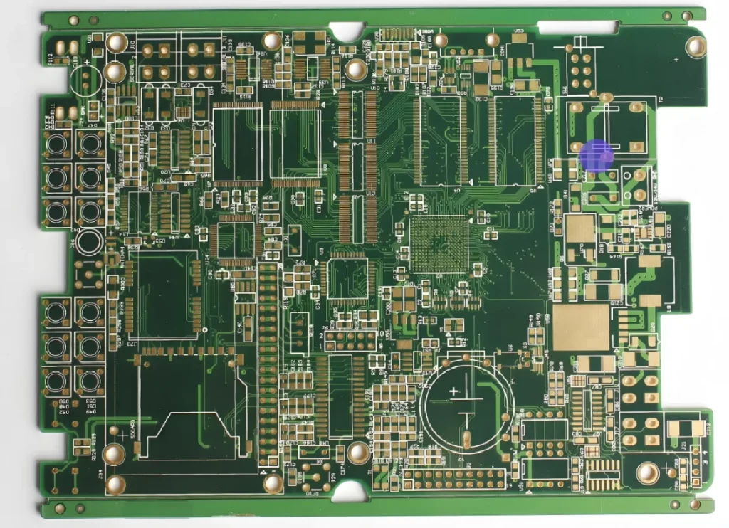
In the electronics manufacturing industry, the introduction of the RoHS standard is not only an environmental requirement, but also a deep-level technological change, especially for the PCB (printed circuit board) industry, which has a systematic and strategic impact. The implementation of this standard forces the entire PCB industry chain to undergo a “green reshaping” in compliance with environmental regulations from raw material procurement, process design, equipment selection, to the final delivery of finished products.
Major changes in raw material selection
In traditional PCB production, many materials (such as lead solder, hexavalent chromium resist, etc.) contain harmful substances that are expressly prohibited or restricted by RoHS. The implementation of RoHS has forced PCB manufacturers to find alternative environmentally friendly materials:
Solder replacement: In the past, tin-lead solder, which was mainly 63/37 SnPb, was replaced by lead-free solder (such as SnAgCu) under the RoHS framework. Although these lead-free solders differ in physical properties, melting points and welding windows, the need to meet RoHS standards has driven their rapid commercialization.
Substrate reform: Many traditional boards contain lead stabilizers or brominated flame retardants (such as PBB, PBDE), which are considered potential sources of environmental risks. RoHS has promoted the research and development and application of FR-4 halogen-free boards (such as S1170, S1000H) and other environmentally friendly high-performance materials.
At this stage, RoHS not only reconstructed the material system, but also prompted the supplier system to update, making green environmental protection the basic threshold of the industrial chain.
Challenges and upgrades of processes and processes
The impact of RoHS standards on PCB manufacturing processes cannot be underestimated. Because of lead removal, halogen removal, and reduction of the use of harmful substances, it directly leads to changes in process parameters, equipment, and test methods:
Changes in soldering temperature: The melting point of lead-free solder is higher (about 217–227°C), which requires reflow soldering, wave soldering and other equipment to withstand higher temperatures, and puts higher requirements on the thermal stress tolerance of PCBs.
Innovation in surface treatment technology: The original common lead-containing tin spray (HASL) has been replaced by environmentally friendly surface treatments such as lead-free tin spray, immersion gold, and OSP. This not only changes the appearance and storage life of the board, but also affects the welding performance during the assembly process.
Evolution of residues and cleaning technology: The ingredients of some lead-free fluxes and cleaning agents are also subject to RoHS constraints, and the cleaning method has gradually shifted from solvent-based to water-based, with higher requirements for equipment and environmental protection.
RoHS has brought about a change in “manufacturing philosophy” at this level: no longer taking cost and output as the only goal, but regarding “environmental compliance” as one of the core competitiveness of the enterprise.
Fluctuation of cost structure
Although RoHS was originally intended to be environmentally friendly, its impact on PCB manufacturing costs was significant in the early stages:
Rising raw material costs: Environmentally friendly materials are generally more expensive, especially when the policy was first implemented, the supply of substitutes was tight and prices fluctuated violently.
Increased equipment investment: In response to the demand for lead-free soldering and halogen-free processes, companies need to update a series of equipment such as reflow ovens, wave soldering, AOI/X-ray inspection systems, etc.
Increased quality control costs: High-temperature processes are prone to new quality problems such as interlayer separation, copper foil blistering, and pad detachment, requiring more testing and R&D resources.
However, with the maturity of the industrial chain and the stability of the technical route, the cost has gradually become reasonable, and even the overall supply chain efficiency has been improved due to standardization.
Promoting the standardization and internationalization of the industry
The implementation of RoHS is not only a legal issue in a single European region, but has gradually become a “common rule” for the global electronics manufacturing industry. Its impact goes far beyond environmental protection:
Raised the entry threshold of the entire PCB industry: Enterprises must establish a systematic material control system (such as BOM banned substance monitoring, MSDS data filing), compliance testing mechanism (such as XRF testing, ICP analysis), etc., in order to participate in international order competition.
Strengthened traceability management and corporate responsibility: RoHS emphasizes the controllability of enterprises over every link in the supply chain, promotes the development of ERP systems, environmental databases, and compliance reporting platforms, and improves the overall management capabilities of enterprises.
Promoted the development of green certification systems: The implementation of RoHS has also spawned new standards such as REACH, WEEE, halogen-free labeling, and UL environmental certification, which work together with RoHS to build a systematic green manufacturing evaluation system.
It can be said that RoHS has made the PCB industry move from “traditional manufacturing” to “responsible manufacturing” and “sustainable manufacturing”, and promoted the industry to develop in the direction of high standards and globalization.
Types and characteristics of HASL process
HASL (Hot Air Solder Leveling) is a traditional and widely used PCB surface treatment process. It can be divided into two main types according to its application method: lead HASL and lead-free HASL. They have their own characteristics in terms of environmental protection, solderability, cost, etc., and we will explain them one by one below.
Lead HASL (Lead HASL)
This is the oldest HASL method. Its main components are tin (Sn) and lead (Pb), and the common ratio is Sn63/Pb37. This ratio has good melting point stability (about 183°C) and excellent wettability, so it has the following characteristics:
Advantages:
Mature and stable process flow, easy to control;
Excellent solderability;
Low cost.
Disadvantages:
Contains lead, does not meet environmental standards such as RoHS;
Potential hazards to the environment and human body;
Restricted or prohibited in some markets (such as the EU).
Lead-free HASL
As environmental regulations become increasingly stringent, more and more PCB manufacturers are turning to lead-free HASL processes. Its mainstream components are alloys such as Sn-Cu, Sn-Ni, Sn-Ag-Cu, etc., which usually have a high melting point (above 217°C), and require more experience in processing and control.
Advantages:
Meets environmental standards such as RoHS;
More suitable for export to Europe and the United States and other regions with high environmental requirements;
Can avoid lead pollution.
Disadvantages:
High melting point, greater thermal stress on PCB boards and components;
Higher process control requirements;
Slightly inferior to lead HASL in solderability;
Slightly higher cost.
General characteristics of HASL process
Whether it is lead-free or lead-free, HASL process has the following common characteristics:
Good solderability: the metal tin layer has good wettability;
Mature operation: widely used in traditional process production lines;
Applicable to through-hole and large-pitch SMT components;
General surface flatness: there are certain challenges for fine lines and dense-footed devices.
In modern high-density and miniaturized PCBs, HASL is gradually replaced by ENIG, OSP and other processes due to its poor flatness, but it is still widely used in the field of low-cost, general electronic products.
Detailed explanation of HASL process flow
Dip soldering and hot air leveling (Hot Air Leveling)
After the solder covers the copper surface, the circuit board will be quickly sent to the hot air leveling equipment. The key to this process is to use one or more pairs of high-pressure hot air nozzles to blow off the excess solder so that it forms a flat and uniform covering layer on the pad.
The temperature of hot air is usually around 250°C and has a certain pressure. The purpose is to shape the molten solder into a standard thickness without damaging the pad or mask. This process requires extremely high equipment control accuracy and must avoid the generation of tin bridges or solder wire drawing.
Cooling and solidification
After the hot air leveling is completed, the board will be cooled quickly to quickly solidify the solder and form a dense and firm solder joint. This cooling step needs to be properly controlled. Too fast may cause the solder to crack, and too slow may cause uneven solder layers.
Post Cleaning
Solder and flux residues will remain on the board surface during the HASL process, especially when using rosin-containing flux. In order to ensure subsequent mounting and reliability, the circuit board needs to be thoroughly cleaned by special cleaning equipment, and sometimes deionized water and cleaning agents are required.
Quality Inspection
After completing HASL, the PCB needs to undergo appearance inspection and thickness testing. Use a microscope to observe the pad coverage, confirm defects such as no tin bridges, bubbles, and voids, and use XRF and other equipment to detect whether the solder thickness meets the IPC standard (such as IPC-6012 stipulates that the HASL surface thickness is ≥1µm).
Packaging and warehousing
Qualified PCBs will be dried and packaged with vacuum bags, desiccants, etc. for moisture and oxidation prevention, and then marked and put into storage, waiting for shipment or entering the PCBA mounting stage.
Technical difficulties and challenges of HASL process
Although HASL process is still widely used in PCB manufacturing due to its maturity and cost advantages, it faces many technical difficulties and challenges in modern electronic manufacturing, especially in the context of high density, high precision and increasingly stringent environmental protection requirements.
Difficulty in controlling solder thickness
The thickness of the solder layer in the HASL process directly affects the subsequent mounting quality and circuit performance. Too thick solder may cause problems such as solder joint bridging and short circuit, especially when mounting fine-pitch components (such as QFP, BGA, etc.); while too thin solder may cause poor solder joints and poor conductivity. During the hot air leveling process, parameters such as wind pressure, temperature, and solder soaking time need to be precisely controlled. Any slight deviation will cause quality problems.
Great influence on thermal stress of PCB substrate
During the HASL process, PCB needs to undergo high-temperature solder soaking and hot air leveling, and the temperature often exceeds 250 degrees Celsius. For high-rise boards, multi-layer boards, or circuit boards using special materials (such as high TG boards), thermal stress may cause board warping, interlayer peeling, or reduced insulation performance. Especially in fine line width and fine pitch designs, thermal stress is more likely to cause manufacturing defects.
Not suitable for ultra-fine pitch and tiny pads
As the trend of miniaturization of electronic products intensifies, the application of micro-pitch chips and micro-pads is increasing. The surface of HASL is relatively uneven, and there is a certain thickness fluctuation in the solder layer, which may cause excessive or insufficient solder when soldering small pads and micro components, reducing welding reliability.
Environmental regulations and waste disposal
Although leaded HASL has a mature process and low cost, it faces increasingly stringent environmental regulations worldwide due to the lead element, such as the EU RoHS directive. Although lead-free HASL meets environmental protection requirements, the process is complex and the cost is increased. In addition, the waste generated by the HASL process (such as solder slag, flux residue, etc.) also needs to be properly handled, which increases the environmental burden.
Flux residue problem
The flux used in the HASL process may leave residues on the PCB surface. If it is not thoroughly cleaned, it may affect the subsequent mounting, welding and electrical performance, and even cause product failure. In particular, some lead-free fluxes have high viscosity, which makes cleaning more difficult.
Advantages and limitations of HASL surface treatment
HASL (hot air leveling) is a classic and widely used PCB surface treatment method. It has low cost, good solderability, and mature manufacturing process, so it occupies an important position in the manufacture of traditional electronic products. However, with the development of miniaturization and high density of electronic products, HASL has also shown certain limitations in some application scenarios. Let’s analyze its main advantages and limitations in detail:
Advantages:
Good solderability
HASL provides uniform and stable tin layer protection, which makes the pad surface have excellent wetting properties. This results in high soldering reliability during SMT (surface mount technology) and THT (through-hole mounting) assembly.
Wide compatibility
This process can be applied to most PCB materials and various types of circuit boards, especially in single-sided, double-sided and some multi-layer boards.
Cost-effective
Compared with other surface treatment methods (such as ENIG, OSP, chemical silver), HASL process equipment is mature, material cost is low, and maintenance is simple, so it is very popular in cost-sensitive projects.
Strong visibility and easy inspection
The pads treated with HASL show obvious metallic luster, which is convenient for engineers to visually inspect and identify problematic solder joints.
Longer storage period
Compared with organic coatings such as OSP, HASL has a longer shelf life under normal storage conditions and is suitable for PCBs that need to be stored for a long time.
Limitations:
Uneven surface
Although “hot air leveling” can remove excess tin liquid, its essence is still a “coating” coverage, which can easily cause local unevenness of the pads. This may cause welding defects in BGA (ball grid array) or precision device mounting below 0.5mm, which have extremely high coplanarity requirements.
Difficult to use in high-density assembly boards (HDI)
High-density interconnection boards require smooth and fine surface treatment, and the thicker coating of HASL (usually between 1-40μm) is prone to short circuits, tombstones, offsets and other problems, so it is gradually replaced by ENIG, OSP and other processes.
High temperature affects material properties
In the HASL process, the PCB needs to pass through a molten tin furnace (temperature is about 245-265°C), which may cause thermal stress deformation or delamination for some high-frequency and high-speed materials (such as PTFE, LCP, etc.).
Environmental protection requirements are becoming increasingly stringent
Although it hasThere is a lead-free HASL process, but the traditional lead-containing HASL is still restricted in some countries and regions. Under the premise of complying with the RoHS and REACH directives, the lead-free process has gradually become the mainstream, but its welding performance and process window are still inferior to the lead-containing version.
Repeated heating affects welding quality
During wave soldering or rework, if the pad is repeatedly heated, the HASL coating may oxidize or peel off, affecting the welding quality.
HASL is still the main surface treatment method in the current mid- and low-end PCB manufacturing, especially suitable for cost-sensitive projects with low device mounting requirements. However, for high-precision, high-reliability, and high-density assembly electronic products, such as 5G communications, automotive electronics, medical equipment, etc., the limitations of HASL are becoming increasingly obvious, and designers and purchasers should choose the most appropriate surface treatment solution according to actual application requirements.
Summary
With the increasing global environmental awareness and increasingly stringent regulatory requirements, RoHS PCB is no longer an option, but a “pass” to the international market. It not only reflects a company’s commitment to environmental responsibility, but also relates to product compliance and the trust of international customers. From the selection of raw materials to every link of the process, to the final finished product testing, the realization of RoHS compliance requires companies to upgrade their concepts, management and technology.
For PCB manufacturers, RoHS is not a burden, but an opportunity to promote companies to improve quality and global competitiveness. For foreign trade purchases and industry newcomers, understanding the meaning and implementation of RoHS PCB will help make smarter and more sustainable choices.
RoHS is a standard, but also a commitment. In today’s world where environmental protection and technology are developing in parallel, every green circuit board is responsible for the future.