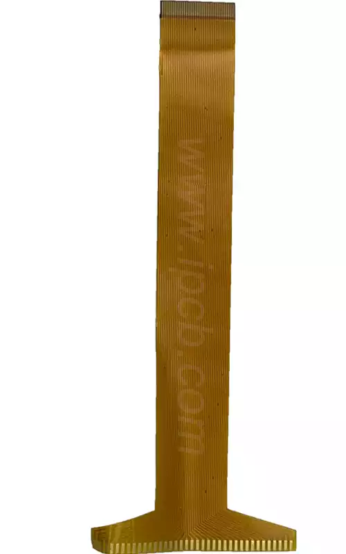
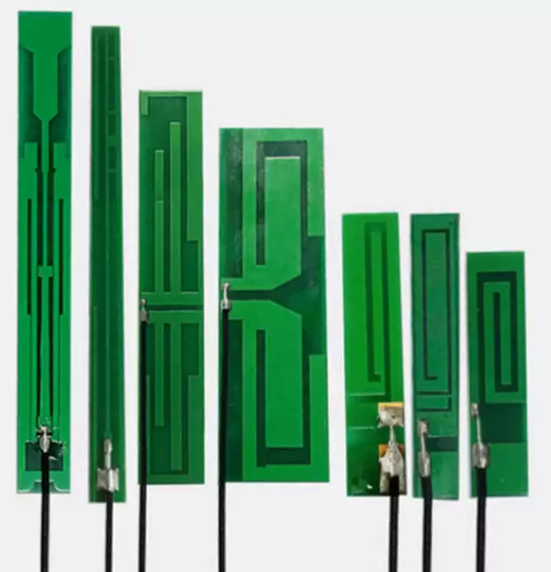
PCB antennas are directly formed by etching metal traces on the PCB substrate to create radiation units, utilizing the rigid material of the PCB for signal transmission and reception, without the need for additional antenna components. Essentially, they are a part of the PCB itself. Their structure is highly flexible, and they can be designed in various forms, such as inverted-F, serpentine, or patch designs, according to the shape of the PCB, space constraints, and frequency band requirements. These antennas integrate seamlessly into the overall PCB layout without the need for additional assembly processes, making them a core source of cost advantages. This also makes them an antenna solution directly controlled by the PCB manufacturing process.
Ceramic antennas are made from high-performance ceramic materials, using processes such as high-temperature sintering and surface metallization. The core advantage is the use of the high dielectric constant of ceramic materials to achieve miniaturization. Common patch-style ceramic antennas can be as small as 2x4mm, making them suitable for extremely compact device spaces. Their structure is relatively fixed, and most are standardized components, which do not require complex on-site design. All that is needed is to reserve the corresponding pads on the PCB for assembly, making ceramic antennas one of the most convenient features in PCB assembly.
The core performance advantages of ceramic antennas lie in miniaturization, frequency stability, and interference resistance. The dielectric constant of the ceramic materials used can range from 20 to 100, which is much higher than that of ordinary FR-4 PCB substrates (around 4.5). This allows the physical size of ceramic antennas to be reduced to 1/5 to 1/10 of traditional antennas at the same operating frequency, making them ideal for devices with extremely limited space, such as TWS earbuds, smartwatches, and mini IoT sensors.
At the same time, the loss tangent of ceramic materials is typically less than 0.001, which ensures an energy conversion efficiency of over 85% in high-frequency operations. Additionally, ceramic materials have a very low coefficient of thermal expansion, maintaining electrical stability in extreme environments from -40°C to +125°C, with a frequency drift rate as low as ±2ppm/°C. The shielding effect of the ceramic casing also enhances the antenna’s interference resistance, making it suitable for applications in automotive electronics, industrial IoT, and other high-stability scenarios, where the performance advantages of ceramic antennas can offset their additional costs.
PCB antennas, on the other hand, excel in bandwidth flexibility and integration. Through clever trace design, they can easily cover multiple frequency bands, such as WiFi 2.4GHz/5GHz and cellular communications, meeting the requirements of various scenarios. Additionally, they can be flexibly adjusted according to the PCB layout to suit different sizes and structures of terminal devices. While their gain is generally lower than that of ceramic antennas (usually 1-3 dBi), it is sufficient to meet the everyday communication needs of consumer electronics.
Since the antenna is an integral part of the PCB, there is no need to worry about alignment issues during assembly, which reduces performance loss caused by improper assembly. PCB antennas are widely used in consumer electronics such as smartphones, routers, and POS machines, where their cost advantages are even more significant.
It is worth noting that the performance of PCB onboard antennas highly depends on the PCB design level and manufacturing process. If the RF design is not optimal, or if the PCB etching precision is insufficient or the clearance area is not reserved properly, issues such as signal attenuation and frequency deviation can occur. In contrast, ceramic antennas, being standardized components, have relatively small performance variations between batches and require lower design and process demands. This indirectly impacts their overall cost and development cycle. PCB manufacturers can further enhance the performance competitiveness of PCB antennas through design and process optimization.
Material Costs: PCB antennas Have an Inherent Advantage
The material cost of PCB antennas is almost negligible. The radiation units are formed by etching copper foil on the PCB substrate, with no additional materials required. The material cost is fully integrated into the PCB substrate cost. The price of a regular FR-4 substrate is about 50-100 yuan per square meter, and when distributed across the antenna part of a single PCB, the material cost is almost negligible. This is a core source of the cost advantage of PCB antennas. In mass production, the material cost of a single PCB onboard antenna can be controlled to less than 0.1 yuan, with almost no increase in the overall material cost of the PCB.
In contrast, ceramic antennas have a more complex manufacturing process, requiring ceramic material preparation, molding, high-temperature sintering, surface metallization, packaging, and testing, all of which demand high production equipment and process precision. This results in higher manufacturing costs. Additionally, since ceramic antennas are independent components, they require separate packaging, transportation, and additional soldering processes during PCB assembly.
This not only increases labor costs but may also lead to defects due to improper soldering, further raising assembly costs. In small-scale production, the combined cost of manufacturing and assembly for a single ceramic antenna can reach 1-5 yuan. For large-scale production (over 100,000 units), this can drop to 0.3-1 yuan, but it still remains higher than PCB antennas. The processing and assembly costs are the key factors in controlling the cost of ceramic antennas.
Development Costs for Ceramic Antennas are Relatively Low
Ceramic antennas are mostly standardized components, so manufacturers can select existing models based on the frequency requirements of terminal devices without investing a lot of research and development resources for design optimization. The testing process is also relatively simple, as it only requires testing parameters such as antenna gain and VSWR to ensure compatibility with the PCB. The development and testing costs can be kept at a low level, which makes ceramic antennas suitable for terminal manufacturers without specialized RF design capabilities. This also lowers the support service costs for PCB manufacturers.
Batch Production Scale Directly Affects the Unit Cost of Both Types of Antennas
The larger the batch production of ceramic antennas, the lower the unit processing and assembly costs. However, due to material costs, the potential for reducing unit costs is limited. On the other hand, PCB antennas do not have significant batch size thresholds, and even in small-scale production, the unit cost can remain low. The larger the batch, the more significant the cost advantage, which is especially evident in large-scale production scenarios with millions of units. This matches well with the scale production needs of the PCB manufacturing industry.
Maintenance Costs in the Future
Ceramic antennas, being independent components, require separate disassembly and replacement if damaged, resulting in higher maintenance costs. Improper soldering may also affect the surrounding PCB traces. In contrast, PCB antennas are integrated with the PCB. If performance issues arise, the entire PCB needs to be replaced. However, due to their very low cost, the overall maintenance cost is lower, and the maintenance process is simpler, making them more suitable for terminal products that require high maintenance efficiency.
Ceramic antennas and PCB antennas are not a matter of “better or worse,” but rather each has its suitable application scenario. The cost difference arises from differences in materials, processing, development, and assembly throughout the entire process, while the performance differences are reflected in how well they meet the requirements of specific scenarios. Ceramic antennas excel in miniaturization and stability, making them suitable for high-end, high-demand scenarios, though they come with a higher cost. PCB antennas excel in low cost, high integration, and scalability, making them suitable for consumer electronics and mass-market scenarios, and they integrate seamlessly with the PCB manufacturing process.