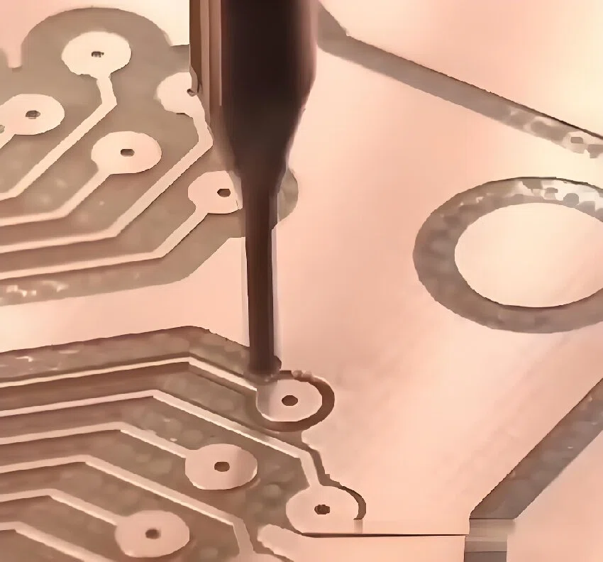
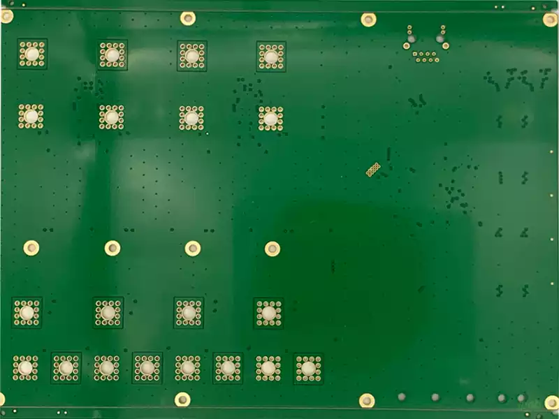
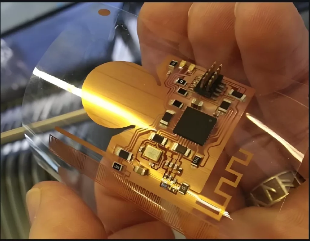
Defect pad smt thermal pad is closely related in the production process. Good smt thermal pad design not only prevents defective pads due to overheating, but also improves the overall weld quality. For example, when a hot pad on a solder joint fails to provide sufficient heat, it can lead to uneven melting of the solder on the pad, which in turn can lead to false soldering or dry soldering. In addition, properly designed hot pads can reduce the uneven temperature caused by the phenomenon of standing monument, which is often found in SMD components and can easily affect the robustness and stability of the final solder.
SMT defect pad refers to the pads that are defective during the SMT process, these defects may affect the connection between the components and the PCB, resulting in unstable or non-functional circuits.
Common causes of defect pad in smt:
‘Monument’ phenomenon, that is, the chip components in the reflow soldering process occurs “vertical”. The ‘monument’ phenomenon is mainly caused by the component ends of the wetting force imbalance, this imbalance leads to the component ends of the moment imbalance, and ultimately make the component ‘stand up’.
Tin beads are a common defect in the reflow soldering process, which not only damages the appearance of the product, but also may lead to bridging and other electrical connection problems. There are two main types of beads: large individual spherical beads that appear next to chip components;and small beads that are scattered around IC pins. The formation of tin beads is mainly caused by several factors:
Bridging is a common defect in SMT (Surface Mount Technology) production,which leads to short circuits between components and must be returned for repair once found.
Core suction phenomenon, also known as suction or core phenomenon,is a common defect in SMT (surface mount technology) soldering, especially in the gas phase reflow soldering process is more common.The phenomenon is manifested in the solder from the pad detachment,along the pin upward flow to the pin and the chip body, resulting in serious soldering problems.
BGA welding bad, BGA that Ball Grid Array (ball grid array package),with its high packaging density,electrical performance and superior cost-effective advantages,and gradually replaced the traditional packaging methods.With the market’s increasing demand for chip integration,the packaging technology of integrated circuits has also put forward more stringent standards.
Cold soldering phenomenon refers to the failure to form a continuous tin tape coverage in the parts of the tin joint, the appearance of which is usually manifested as a rough, dull and tin powder-like particles on the surface (the so-called raw tin bad).
False soldering: is only a small amount of solder at the solder joints, resulting in poor contact lap, electrical testing when on and off. False soldering and false soldering refers to the surface of the weldment is not fully plated on the tin layer, between the weldment is not fixed by the solder, due to the surface of the weldment is not clean or flux with too little caused by.
Empty soldering: The solder joints should be soldered but not soldered. The solder paste is too little, the problem of the parts themselves, the position of the parts, the time after the printing of tin is too long… and so on will cause the empty soldering.
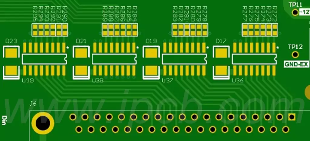
SMT thermal pad are specialised welding machines that work by heating the surface of a metal workpiece to its melting point and then applying pressure to join two or more metal workpieces together. This technology is mainly used for joining and repairing metal materials and is efficient, easy and reliable.
Soldering process for smt thermal pad:
Heating phase: The surface of the metal workpiece is heated precisely until it reaches its melting point by means of a built-in electric heating element or flame heating system.
Pressure application stage: After the metal workpiece is heated to a molten state, the hot pad will apply a certain amount of pressure to promote full contact between the metal workpieces to achieve the purpose of welding.
Cooling and curing phase: After the pressure is applied, the metal waits for natural cooling and curing to form a solid welded connection.
The workflow of smt thermal pad in practice:
Preparation: Firstly, the metal workpiece to be soldered is properly placed on the hot pad and accurately positioned to ensure the accuracy and quality of the soldering.
Initiate heating: The heating unit of the hot pad is then activated to start heating the surface of the metal workpiece until its temperature reaches the melting point.
Applying Pressure: As soon as the metal workpiece reaches the melting point, the hot plate applies a pre-set pressure, which induces a tight contact between the metal workpieces to form a welded connection.
Cooling and Completion: Finally, after the metal parts have cooled and solidified, the heating is stopped and the pressure is released, and the soldering process is complete.
Defect pad on the impact of the smt thermal pad
Reduce the quality of soldering: the existence of defect pad will directly affects the soldering process of heat conduction and solder paste wetting behaviour, resulting in the formation of the hot pad is blocked, which in turn affects the strength of the entire soldered joint and electrical performance.
Increase rework costs: defective pads often need to be repaired through rework, which not only increases production costs, but also may be due to improper operation in the rework process to further damage the pad or component, reducing the overall reliability of the product.
Impact on production efficiency: defective pads lead to testing, rework or even scrap, will extend the production cycle, reduce production efficiency, affecting the competitiveness of enterprises in the market.
Considerations in design
When designing pads, the following factors need to be considered to avoid defect pads and to ensure the effectiveness of hot pads:
Pad size and layout: Ensure that the width of the pad matches the component pins to avoid over-width or over-narrowing, which will affect the quality of the solder joints.
Material Selection: The pad material should have good solderability and thermal conductivity, and surface treatment such as chemical nickel-gold plating or chemical tin plating is usually recommended to enhance the soldering effect.
Thermal management design: In high-power circuits, the layout of the smt thermal pad can be reasonably designed to effectively control the temperature and heat dissipation, to avoid damage to electronic components.
Quality control of defect pad smt thermal pad is the key to ensure the performance of electronic products. Optimised design and strict management is an effective way to prevent defects and improve soldering quality.
