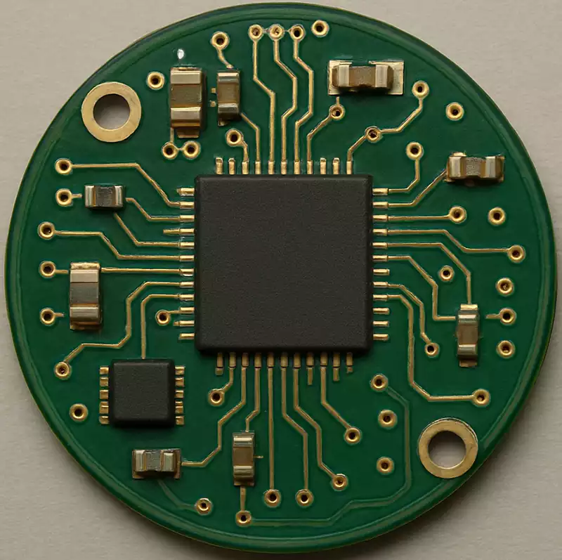
Round PCB boards are printed circuit boards shaped into a circular (or near-circular) form. They share identical electrical functionality with conventional rectangular PCBs, differing primarily in structural configuration and application scenarios.
Structural Components of Round PCB Boards
Substrate: Typically composed of insulating materials such as fibreglass-reinforced epoxy (FR-4), providing mechanical support and electrical insulation for the circuitry.
Copper Foil Layer: Adhered to the substrate surface, it is etched to form various traces and pads. These connect electronic components to facilitate electrical signal transmission.
Electronic Components: Including chips, resistors, capacitors, inductors, etc., these are fixed to pads on the copper foil layer via soldering or similar methods, forming a complete circuit system.
Solder mask and silkscreen layers: The solder mask covers the copper layer to prevent short circuits between traces and protect the copper from oxidation. The silkscreen layer labels component locations, part numbers, and other information for assembly and maintenance.
Advantages of round pcb boards:
Greater Circuit Board Space
A notable advantage of round pcb boards is the provision of increased circuit board space.
Reduced Electromagnetic Interference
The Roundshape aids in minimising electromagnetic interference, particularly in high-frequency applications. With fewer sharp corners and smoother routing paths, round pcb boards enable clearer signal transmission and reduced interference, which is crucial for sensitive or compact devices.
Common Applications of round pcb boards
Medical Devices: Employed in hearing aids, portable displays, and diagnostic tools requiring compact, lightweight circuit boards.
Wearable Devices: Found in smartwatches, fitness trackers, and VR headsets where round designs integrate seamlessly into curved or compact enclosures.
Consumer Electronics: Ideal for round connectors, wireless charging pads, and portable devices demanding both style and functionality.
LED Lighting: Commonly found in ring lights, LED strips, and desk lamps, where round pcb boards support uniform light distribution and superior heat dissipation.
Automotive and Aerospace: Utilised in sensor units, control systems, and lighting where space optimisation and durability in harsh conditions are paramount.
Industrial Automation: Found in customised equipment and modular systems, assisting engineers in designing efficient layouts within confined or unconventional spaces.
Military/Defence: Trusted for high-density electronics in communications, surveillance, and rugged field equipment subjected to extreme environments.
Design Considerations for round pcb boards:
Selecting Suitable CAD Tools
Choose CAD software supporting custom shape design, such as Eagle, Altium Designer, or KiCad. These tools facilitate drawing precise contours, accurately placing components, and managing curved layouts.
Within Eagle software, utilise the miter command to round corners, creating true round pcb board shapes.
Drawing Precise Round Outlines
When drawing round outlines, never attempt freehand drafting. Always employ precise tools to construct round layouts. In Eagle, begin by drawing a square, then utilise the mitre command. Ensure all four sides of the square are of equal length to guarantee the final board is truly circular, rather than elliptical or off-centre.
Planning Component Layout
Given the limited space on round pcb boards, particularly in peripheral areas, position critical components such as chips and connectors as centrally as possible. Allocate smaller or less vital components to the outer regions. This layout promotes overall balance, facilitates soldering operations, and enhances thermal stability.
Optimising Trace Routing
Curved designs present challenges for trace routing. When routing traces, employ smooth paths with controlled angles, avoiding sharp corners. Strive for short, orderly traces with consistent spacing – this is particularly crucial for high-speed or sensitive circuits.
Defining Power and Ground Planes
Employ the polygon editor within CAD tools to shape power and ground planes to match the PCB’s geometry. Thoughtfully designed planes enhance signal stability, optimise thermal management, and reduce electromagnetic interference (EMI). Avoid sharp edges or fragmented fill areas that may cause electrical issues.
Consider manufacturing factors
An excellent design should possess good manufacturability. During design, ensure sufficient clearance between copper layers and board edges. Where possible, use standard dimensions for pads, holes, and layers. The simpler the layout, the higher the product reliability and production efficiency, and the lower the cost.
Round pcb boards, as a specialised form factor, offer distinct advantages in structural matching, space utilisation, electromagnetic performance, and product aesthetics. By selecting appropriate design tools, precisely drafting board shapes, scientifically planning component layouts, and thoroughly considering manufacturing factors, engineers can fully realise the potential of round PCB boards. This enables an optimal balance of performance and cost in practical applications, making them an indispensable choice in modern electronic product design.