Cold solder joints refer to instances during the soldering process where an inadequate metallic bond forms between the solder and the workpiece. While appearing connected, such joints exhibit poor contact, severely compromising the performance and reliability of electronic products and potentially causing product failure. Accurate detection and effective remediation of cold solder joints are crucial for ensuring the quality of PCB boards and related electronic products.
Methods for cold solder joints
Visual Inspection
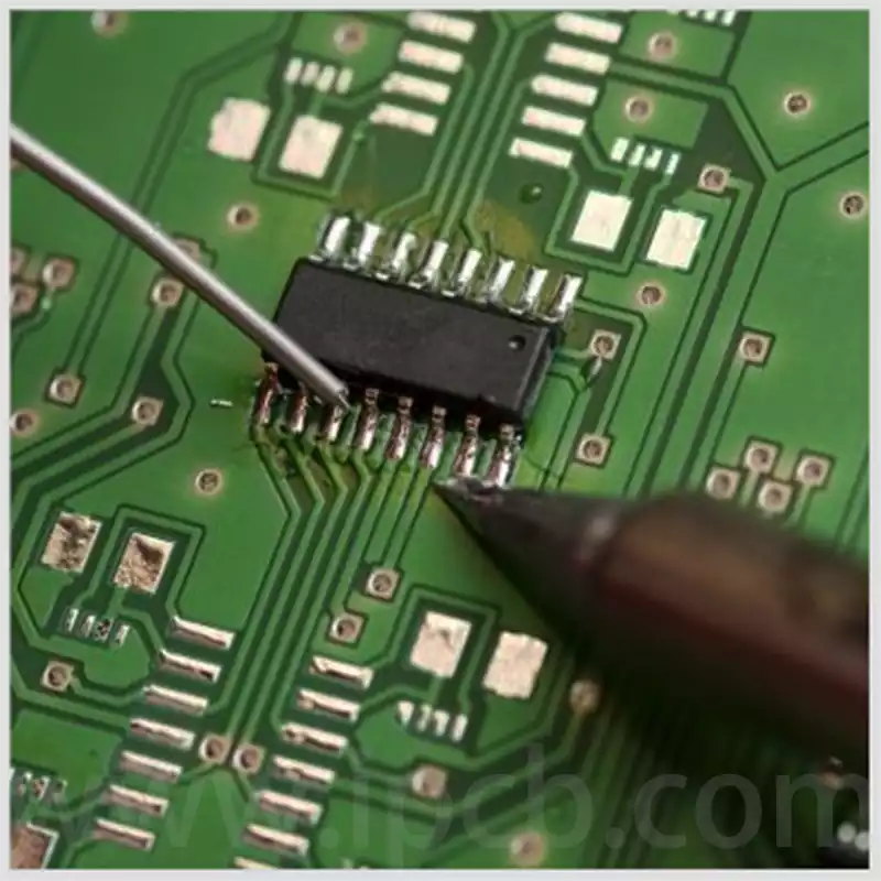
Manual Visual Inspection: This constitutes the most fundamental detection method. Trained technicians utilise tools such as magnifying glasses or microscopes to meticulously examine the appearance of solder joints. Faulty joints typically exhibit a lacklustre, dull appearance, contrasting markedly with the lustrous, rounded finish of sound joints. Additionally, the shape of a faulty joint may be irregular, with uneven solder distribution, and visible cracks or voids may sometimes be observed. For instance, when inspecting solder joints on surface-mount technology (SMT) components, insufficient solder on one side of the joint accompanied by a gap at the interface with the component lead strongly indicates a cold solder joint. However, manual visual inspection is significantly influenced by the inspector’s experience and fatigue levels, potentially leading to missed defects in minute cold solder joint failures.
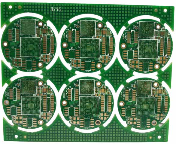
Automated Optical Inspection (AOI): AOI employs optical imaging and image processing technologies to comprehensively scan PCBs. By comparing captured solder joint images against pre-stored standard images, it rapidly detects various defects, including cold solder joints. AOI identifies anomalies in joint parameters such as size, shape, and colour to determine the presence of cold soldering. For instance, when a solder joint’s area falls below the standard value or its edge contour exhibits significant deviation from the reference image, the AOI system issues an alert indicating potential solder joint failure. AOI offers high-speed, high-precision inspection with excellent repeatability, substantially enhancing detection efficiency. However, its effectiveness may be limited for joints concealed beneath components or within multilayer PCBs.
Electrical Performance Testing
Flying Probe Testing: Flying probe test equipment uses movable probes to contact test points on the PCB, assessing circuit continuity. During testing, the probes sequentially contact both ends of the solder joint, measuring its resistance value. If a solder joint is faulty, the resistance value will increase significantly due to poor contact, or may even indicate an open circuit. Flying probe testing enables precise inspection of individual cold solder joints, making it suitable for small-batch, multi-variety PCB testing. However, its relatively slow testing speed results in lower efficiency for mass-produced PCBs.
ICT In-Circuit Testing: ICT (In-Circuit Test) is a comprehensive electrical performance testing method applied to components and circuits on the PCB after assembly. Using specially designed test fixtures, it ensures close contact between test probes and PCB test points to verify solder joint electrical connections. ICT simulates circuit operating conditions, testing solder joint conductivity under varying voltage and current conditions. When solder joints exhibit poor soldering, ICT detects electrical anomalies such as signal transmission interruptions or excessive voltage drops. ICT offers rapid testing speeds and high accuracy, capable of covering the majority of cold solder joints on a circuit board. However, the production cost of test fixtures is relatively high, and manufacturing them presents significant challenges for high-density, fine-pitch PCBs.
Physical Inspection
X-ray Inspection: X-rays possess the ability to penetrate objects. X-ray inspection technology leverages this property to examine the internal structure of PCBs. An X-ray source emits radiation that passes through the PCB, with a detector on the opposite side receiving the transmitted rays. By analysing the degree of attenuation and imaging patterns, it determines whether solder joints exhibit cold soldering. Cold solder joints typically contain voids or gaps internally; these defects cause X-rays to attenuate differently during transmission compared to sound joints, manifesting as abnormal grey-scale variations in the X-ray image. For instance, in multilayer PCBs, X-ray inspection can clearly reveal the internal structure of solder joints hidden within inner layers, enabling accurate detection of cold solder joints. While X-ray inspection can identify internal defects invisible to the naked eye, it involves higher equipment costs and relatively slower inspection speeds.
Acoustic Microscopy (SAM): SAM utilises the propagation characteristics of ultrasonic waves through different media to assess solder joint quality. When ultrasonic waves are emitted onto the PCB, reflection, refraction, and transmission occur at the interface between the cold solder joints and surrounding materials. If a cold solder joint is present, internal voids or poorly bonded areas alter the propagation path and reflection patterns of the ultrasonic waves. By receiving the reflected ultrasonic signals and converting them into images, SAM clearly displays the internal structure of the solder joint. Solder joints with cold solder joints exhibit distinct contrast and morphological characteristics in SAM images compared to normal joints. SAM inspection offers high sensitivity to minute internal defects, though the equipment is costly and the process relatively complex.
The analysis of cold soldering causes and procedures may be conducted in the following sequence:
(1) First inspect the solder joint interface for contaminants such as rust or oil residues, or for uneven surfaces and poor contact. Such issues increase contact resistance, reduce current flow, and prevent the solder joint interface from reaching adequate temperatures.
(2) Verify whether the overlap dimension of the solder joint is correct, checking for reduced overlap or cracking on the drive side. Reduced overlap diminishes the bonding area between preceding and succeeding steel strips, decreasing the total load-bearing surface and compromising its ability to withstand significant tension. Cracks on the drive side, in particular, cause stress concentration, leading to progressively larger fractures and eventual rupture.
(3) Verify whether the current setting complies with process specifications. Ensure the current setting increases proportionally with changes in product thickness; failure to do so results in insufficient welding current and poor weld quality.
(4) Verify welding wheel pressure is appropriate. Insufficient pressure increases contact resistance, reducing actual current flow. Although the welding controller employs constant-current mode, resistance increases beyond a certain threshold (typically 15%) may exceed current compensation limits. Current cannot then rise proportionally with resistance, failing to reach the set value. Under such conditions, the system will issue an alarm during normal operation. In practical operation, if the precise cause of cold soldering cannot be immediately identified, clean the ends of the steel strip thoroughly, increase the overlap length, and appropriately raise both the welding current and wheel pressure before re-welding. Closely monitor the formation of the weld seam during this process; in most instances, this emergency procedure will resolve the issue. Naturally, should control system faults or mains voltage fluctuations cause cold soldering, alternative measures must be implemented.
Methods for resolving cold solder joints in pcb boards
- Enhance quality control. During manufacturing, strengthen quality control over materials and processes, strictly adhering to operational requirements for soldering. Pay particular attention to soldering temperature, duration, and speed to ensure soldering quality.
- Adjust soldering temperature and duration. During soldering, configure appropriate temperature and time settings based on the board material and equipment used. This prevents cold soldering caused by insufficient temperature or inadequate duration.
- Employ reliable soldering equipment. Select dependable soldering apparatus that meets required power and precision specifications, ensuring stability and durability.
- Enhance soldering personnel skills. During circuit board manufacturing, strengthen training for soldering operatives to improve their operational proficiency and self-inspection capabilities.
Cold solder joint severely compromises electronic product performance, with diverse detection methods available. To effectively address this issue, a multi-faceted approach is required, encompassing manufacturing quality control, adjustment of soldering parameters, equipment selection, and workforce skill enhancement. The integrated application of these strategies is pivotal to ensuring high-quality and reliable electronic products.