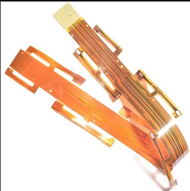
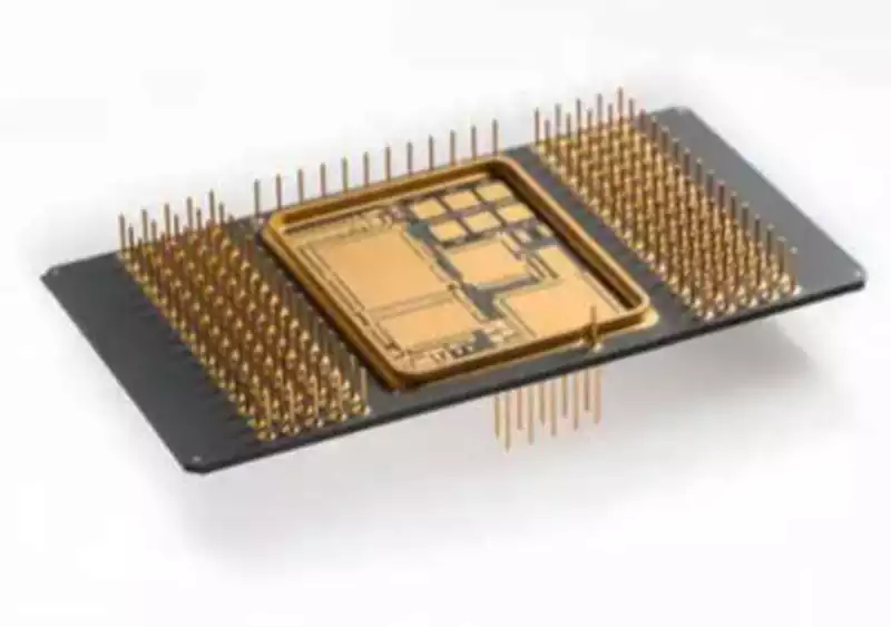
The package substrate comprises both the carrier for electronic circuits (i.e., the substrate material) and the copper electrical interconnect structure (encompassing electronic circuits, through-holes, and other components). The quality of this electrical interconnect structure directly impacts the stability and reliability of signal transmission within integrated circuits, thereby determining whether the functional design of electronic products can be properly realised. Package substrates fall within the category of specialised printed circuit boards, serving as the fundamental component that connects high-precision chips or devices to printed circuit boards of comparatively lower precision.
In the early 20th century, Paul Eisler first proposed the concept of ‘printed circuits’ and successfully developed the world’s first Printed Circuit Board (PCB). With the advent of semiconductor chips, integrated circuit packaging substrates emerged as a distinct category within the printed circuit board family, becoming a specialised type of printed circuit board. Its primary function is to establish electrical interconnection pathways between the integrated circuits within the chip and external electronic circuits.
The role of integrated circuit package substrates in electronic packaging engineering
As a supporting structure, the package substrate protects the semiconductor components within the chip. It facilitates electrical connections between the electronic circuits of the integrated circuit functional modules within the chip and external functional components. It provides a stable support structure and thermal dissipation pathways for the chip’s functional components, while also serving as an assembly platform for mounting other electronic components. Furthermore, packaging substrates facilitate multi-pin integration in ICs, reduce package dimensions, enhance electrical and thermal performance, and enable ultra-high density or multi-chip modularisation.
An Overview of Three Development Stages for Packaging Substrates
Presently, packaging substrates may be regarded as PCBs (printed circuit boards) possessing enhanced performance or specialised functions. They fulfil multiple roles including electrical interconnection, protection, support, thermal dissipation, and assembly for chips and electronic components. Capable of enabling multi-pin configurations, reducing package size, improving electrical and thermal performance, achieving ultra-high density or multi-chip modularisation, and offering high reliability, they constitute a vital electronic substrate.
Primary Classification Structure of Package Substrates
Currently, the package substrate industry lacks a unified classification standard. Substrates are generally categorised based on material composition and manufacturing techniques.
From a material perspective, package substrates are divided into inorganic and organic substrates. Inorganic substrates primarily encompass ceramic-based and glass-based substrates; organic substrates mainly include phenolic, polyester, and epoxy resin substrates.
Based on manufacturing methods, substrates can be categorised as core-type substrates and newer coreless substrates.
Core-type substrates feature a two-part structural composition: a central core layer flanked by laminated layers above and below. Their manufacturing process is fundamentally derived from high-density interconnect (HDI) printed circuit board technology, subsequently refined and optimised.
Coreless substrates, also termed non-core substrates, refer to packaging substrate types where the core layer has been removed. The fabrication of new coreless packaging substrates primarily employs bottom-up electroplating techniques to construct interlayer conductive structures—copper pillars. Utilising only build-up layers and copper layers, it achieves high-density routing through a semi-additive process (SAP) lamination technique.
Core Functions and Structural Characteristics of Packaging Substrates
The core function of packaging substrates lies in achieving electrical interconnection between integrated circuit chips and external circuits or electronic components.
Core-based packaging substrates comprise a core board and outer layer circuits, featuring interconnect structures including buried vias, blind vias, through-holes, and conductive traces. In contrast, core-less packaging substrates primarily utilise copper pillars and traces for interconnection. The technical distinction in coreless substrate fabrication lies in employing bottom-up copper electroplating to construct the interconnect structure—copper pillars and traces. Compared to buried and blind vias, copper pillars are solid cylindrical copper structures offering superior electrical transmission performance. Their dimensions are significantly smaller than blind vias, typically measuring around 40μm in diameter.
Differences between Package Substrates and PCBs
A package substrate is an electronic substrate that provides electrical connections, protection, support, thermal dissipation, and assembly functions for chips and electronic components. Through these capabilities, it enables multi-pin configurations, reduces the volume of packaged products, enhances electrical performance and thermal management, achieves ultra-high density or multi-chip modularisation, and delivers high reliability.
Simply put, packaging substrates can be regarded as PCBs (printed circuit boards) or thin/thick-film circuit substrates with enhanced performance or specialised functions. The packaging substrate facilitates electrical interconnection and transition between different circuits on the chip and conventional printed circuit boards (typically motherboards, daughterboards, backplanes, etc.), while also providing protection, support, thermal management, and assembly capabilities for the chip.
Distinction between PWB and PCB
PWB (printed wiring board): Refers to an insulating substrate with conductor patterns arranged on its surface and internally. A PWB is a semi-finished product primarily functioning as a substrate for mounting electronic components. Through conductor routing connections, it forms unit electronic circuits to realise its circuit functionality. PCB (printed circuit board): This denotes the complete PWB substrate with mounted electronic components. In most contexts, PWB and PCB are treated as synonymous terms without distinction. In practice, distinctions exist in certain contexts. For instance, PCB may sometimes specifically denote a complete circuit formed by purely printed means on an insulating substrate, capable of independent operation and incorporating electronic components. Conversely, PWB places greater emphasis on its function as a carrier for mounted components, either constituting an assembled circuit or forming part of a printed circuit board assembly. Both are commonly abbreviated as printed boards.
Motherboard: Also termed the mainboard. This is an electronic substrate mounted with various active and passive electronic components on a larger PCB, enabling interconnection with daughterboards and other devices. Within the telecommunications industry, it is generally referred to as a backplane.
Substrate: A printed circuit board designed to carry various active and passive electronic components, connectors, units, daughterboards, and other diverse electronic devices. Examples include package substrates, substrate-like PCBs, various standard PCBs, and final assembly boards.
Substrate-Like PCB (SLP): As the name implies, this is a PCB resembling substrate specifications. Originally classified as an HDI board, its specifications now approach those of substrates used for IC packaging. SLPs remain a type of rigid PCB but employ manufacturing processes closer to semiconductor standards. Currently, SLPs require line width/spacing of ≤30μm/30μm, precluding subtractive manufacturing methods and necessitating the use of MSAP (Micro-Structure Additive Process) technology. They integrate the functions of both packaging substrates and carrier boards, though their manufacturing processes, raw materials, and design approaches (single-piece or multi-piece) remain to be finalised. Substrate-like boards emerged as a result of Apple’s new smartphone developments. The iPhone 8 in 2017 first employed HDI boards resembling substrate-like boards, manufactured using processes akin to IC production, enabling a slimmer, lighter, and more compact phone design. The substrate material for substrate-like boards is similar to that used in IC packaging substrates, primarily consisting of BT resin CCL and ABF resin laminated dielectric films.
As LSI (Large Scale Integration) density increases, signal transmission speeds accelerate, and electronic devices pursue ever-slimmer profiles, reliance on single- or double-sided conductor routing alone becomes insufficient. Furthermore, co-locating power lines, ground planes, and signal traces within the same conductor layer imposes significant constraints, severely limiting routing flexibility. Dedicated power planes, ground planes, and signal layers, positioned within the inner layers of a multilayer board, not only enhance routing flexibility but also mitigate issues such as signal interference and electromagnetic radiation. This requirement has further driven the development of multilayer substrates. Consequently, PCBs have integrated key electronic packaging technologies and play an increasingly vital role. It can be said that contemporary PCBs represent the culmination of multiple modern technologies.
HDI Substrates: Typically manufactured using the build-up method, where the number of layers increases the technical sophistication of the board. Standard HDI boards generally employ a single build-up layer, while high-end HDI boards utilise two or more layers, alongside advanced PCB techniques such as stacked vias, electroplated via filling, and laser direct drilling. High-end HDI boards are primarily deployed in 4G mobile phones, high-end digital cameras, IC carrier boards, and similar applications.
With continuous technological advancement, the role of packaging substrates in electronic products grows ever more critical, particularly within integrated circuit packaging. They not only facilitate effective electrical connections between chips and external circuits but also enhance product functionality, reliability, and thermal management. Looking ahead, as electronic devices demand ever-higher integration, transmission speeds, and slimmer profiles, packaging substrate technology will continue evolving towards greater performance, multifunctionality, and higher density. For the semiconductor industry, packaging substrates will become one of the key technologies ensuring efficient chip operation and seamless electronic device functionality.