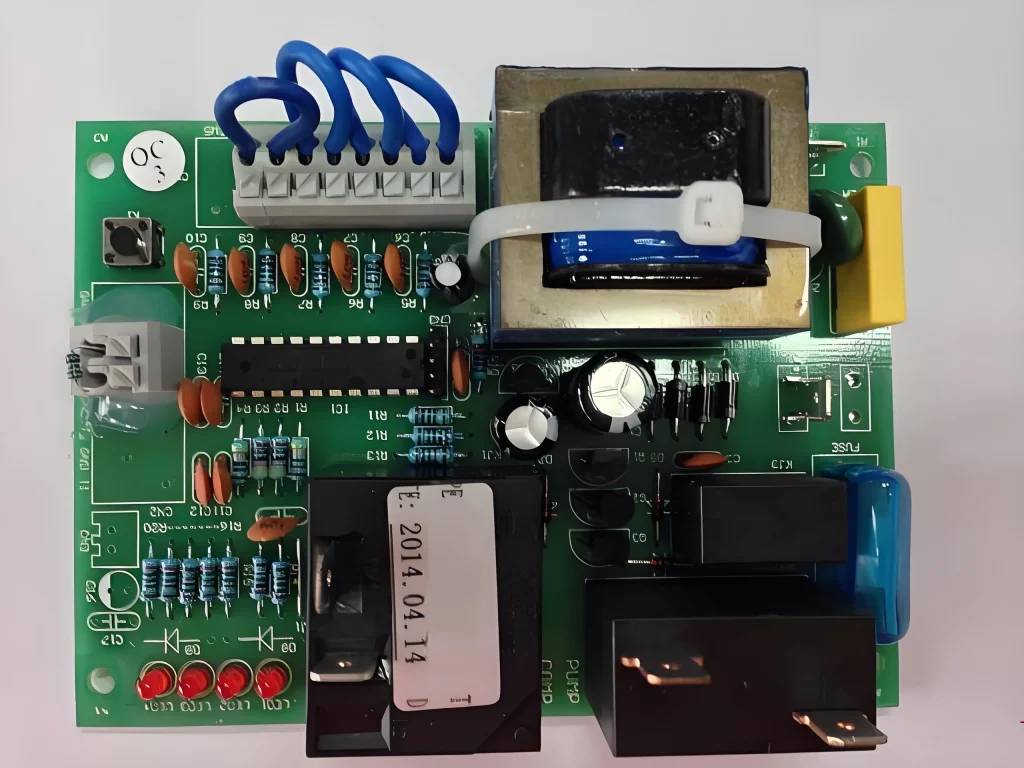
As electronic products demand increasingly diverse functionalities, pcb board structures have grown ever more complex. Constrained by spatial limitations, PCB circuit boards have progressively “evolved” from single-layer to double-layer and ultimately multi-layer designs. What, then, distinguishes the manufacturing processes of multi-layer PCB boards from those of double-layer PCBs?
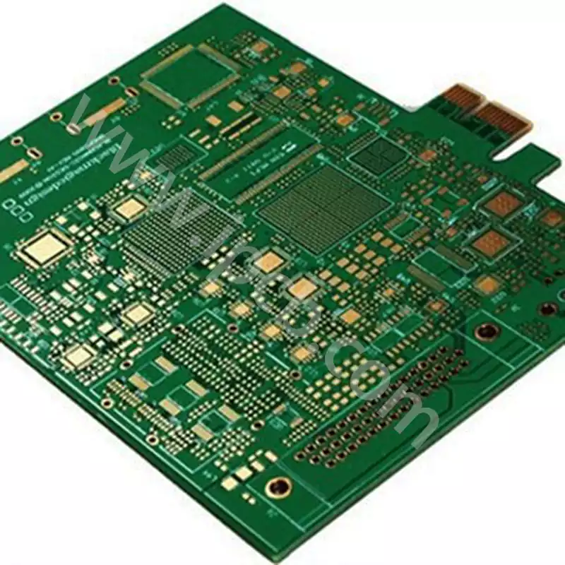
A multilayer pcb board is a type of printed circuit board formed by laminating and bonding alternating layers of conductive patterns and insulating materials. It comprises three or more layers of conductive patterns, with electrical interconnections between layers achieved through plated-through holes. By employing a double-sided board as the inner layer with two single-sided boards as outer layers, or conversely using two double-sided boards as inner layers with two single-sided boards as outer layers, these layers are laminated together using a positioning system and insulating adhesive. Conductive patterns are then interconnected according to design specifications, resulting in four-layer or six-layer printed circuit boards, also termed multilayer PCB boards.
Multilayer circuit boards are typically manufactured using epoxy glass cloth laminated with copper foil. Their production process evolved from the technology used for plated-through-hole double-sided boards. The standard process involves first etching the inner layer pattern, followed by blackening treatment. Pre-designed laminates are then added with prepreg sheets before copper foil is applied to both surfaces. This assembly is pressed under heat and pressure to produce a ‘double-sided copper-clad laminate’ with the inner layer pattern prepared. Subsequently, CNC drilling is performed according to the pre-designed positioning system. Post-drilling, the hole walls undergo etching and deburring before proceeding with the double-sided plated-through-hole printed circuit board process.
Structural Differences: Layer Count and Design Complexity
Double-layer boards:
- Contain only two conductive layers (top and bottom) with an insulating substrate (e.g., FR-4) between them. Interlayer connections are achieved through drilling and copper plating.
- Typically 1.6mm thick, with trace widths generally ≥0.2mm (referencing IPC-2221 standards).
- Simple design, suitable for low-density circuits such as power modules and LED light boards.
- Constructed from four or more conductive layers (commonly 4-12 layers, with high-end variants reaching 50 layers). Layers are bonded using prepreg (PP sheets) and interconnected via blind/buried via technology.
- Thickness increases proportionally with layer count (e.g., 4-layer boards approx. 0.8-1.2mm, 8-layer boards 1.6-2.4mm).
- Supports high-density routing with trace widths down to 0.1mm, suitable for complex applications like CPU motherboards and 5G communication equipment.
Performance and Application Scenarios Comparison
Signal Integrity:
- Double-layer boards suffer significant interlayer interference, prone to crosstalk in high-frequency signals (suitable for frequencies <100MHz).
- Multilayer pcb boards isolate noise via ground planes, supporting GHz-level high-frequency signals (e.g., PCIe 4.0 at 16GT/s).
Mechanical Strength and Heat Dissipation:
- Multilayer pcb boards exhibit 30%-50% higher bending strength (source: IPC-6012 standard) due to additional copper layers and insulating materials, with heat dissipation facilitated by inner copper planes.
Typical Applications:
- Double-layer boards: Low-cost products like home appliance control boards and toy circuits.
- Multilayer boards: Smartphones (6-8 layers), server motherboards (12+ layers), aerospace equipment (high reliability requirements).
Compared to double-sided boards, multilayer printed circuit board production incorporates several unique steps: inner layer imaging and blackening, lamination, etching, and drill residue removal. While similarities exist in certain process parameters, equipment precision, and complexity, multilayer boards impose higher demands across multiple aspects. For instance, inner layer metallisation connections are critical for reliability, necessitating stricter hole wall quality standards and presenting greater challenges for drilling processes. Furthermore, parameters such as the number of stacked boards during drilling, drill bit rotational speed, and feed rate differ from those for double-sided boards. Concurrently, the inspection procedures for both finished and semi-finished multilayer boards are more rigorous and complex. Owing to their intricate structure, a glycerine hot-melt process with uniform temperature distribution is required to ensure product quality and prevent potential process issues arising from localised excessive temperature rise.
Multilayer pcb boards exhibit significant manufacturing process differences from double-layer boards, primarily in inner layer processing, lamination techniques, and post-treatment stages. Multilayer board production first requires etching and blackening of inner layer conductive patterns to enhance insulation properties and interlayer bonding strength. Subsequently, layers are bonded together into a unified structure using positioning systems and prepregs (pre-impregnated materials), contrasting sharply with the double-layer process where patterns are formed directly on both sides of the substrate.
Hole processing and post-treatment demands stricter requirements for multilayer circuit boards. Following drilling, multilayer boards undergo undercut etching and deburring to ensure hole wall cleanliness and subsequent metallisation layer adhesion, which is critical for electrical interconnections between layers. Furthermore, multilayer pcb boards involve more complex and precise drilling parameters (such as stack-up count, drill speed, feed rate) and inspection procedures for both finished and semi-finished products compared to double-layer boards, ensuring the reliability of the final product.