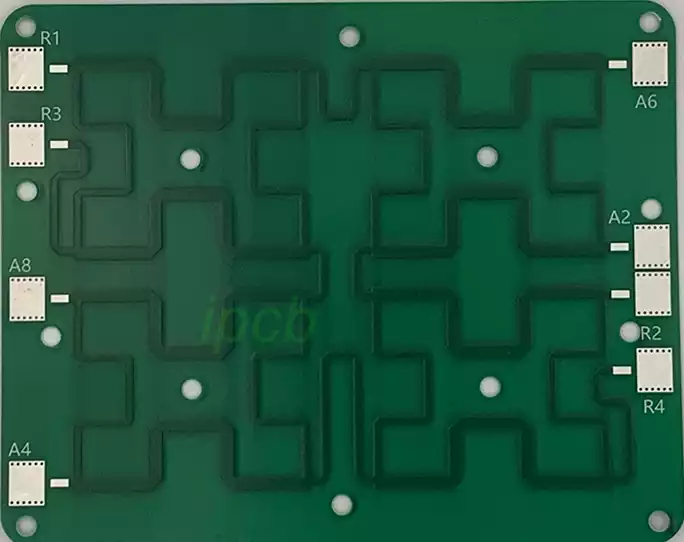
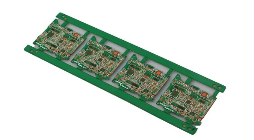
A double sided PCB board is an electronic component carrier consisting of an insulated substrate and a metal conductive layer. It has two working layers that can be used for wiring and assembling electronic components, i.e. the top layer and the bottom layer. These two layers are connected by means of holes to form an electrical connection. The conductive layer of a double-sided PCB board is usually copper foil, which is chemically etched or mechanically stripped to form the desired circuit pattern.
Double-sided PCB boards can accommodate more complex circuit designs for different applications. It has good reliability, stability and durability for efficient transmission of current and signals. Double-sided PCB boards are widely used in a variety of applications, including communications, computers, industrial controls and consumer electronics.
Double-sided PCB board compared with single-sided PCB board:
1. There are board thickness, such as 0.8MM.1.0.1.2.16.2.0, there are customized 3.0MM, 4.00MM customized products, according to the needs of the product, different materials;.
2. Single and double-sided circuit boards have flame retardant grade, such as FR4, is flame retardant 4, flame retardant grade is common to single and double PCB boards.
3. Single-sided PCB board manufacturing simple, less process, double-sided PCB board manufacturing process to be more, wash the board, in accordance with the requirements of electrical products, open PCB board size, single-sided PCB board printing line, over the machine brush out the line, that double-sided board to play empty, after the copper to sink, the high-end to sink the gold, single-panel printing oil, the oven oven, a large amount of molds punching board, a small amount of machine gongs out of the board, molding on shipment. Double-sided PCBA, more processes, double-sided printing, over the line out, print protection green oil, high Rui sinking gold (sinking gold, the cost of high), spray tin (low cost, high dosage), antioxidant (lower cost), weldability, sinking gold is the most solid. Open stamping molds, or machine gong boards.
4. Single-sided PCB boards used in the lowest-end electrical products, double-sided PCB boards used in high-end appliances, double-sided PCB boards cost a little higher. The difference between double-sided PCB board and single-sided PCB board is that the single-sided panel line is only on one side of the PCB board, while the line of the double-sided PCB can be in the two sides of the PCB board, the middle of the PCB board with a hole in the middle of the line will be connected to the double-sided PCB board. Parameters of double-sided PCB board double-sided PCB board production and single-sided PCB board in addition to the production process is not the same, but also more than one copper sinking process, that is, the double-sided line conduction process.
Double-sided PCB board production process
1. Design: According to the circuit schematic wiring design, determine the location of components and wiring path.
2. Printing: The designed circuit pattern is transferred to the copper foil through photolithography to form the circuit pattern.
3. Drilling: According to the design requirements, drilling holes on the circuit board for the installation of components and wiring.
4. Copper plating: Through chemical copper plating or electrolytic copper plating, a conductive layer is formed at the drilled holes.
5. Pattern: Remove unwanted copper foil by etching or stripping to form circuit patterns.
6. Soldering: Components are soldered to the board to complete the circuit.
Double sided PCB board, with its excellent circuit design capacity, high reliability and wide range of applications, has become an indispensable and important component in the modern electronic industry. Every process from design to production reflects precision craftsmanship and rigor. Whether it is communication, computer, or industrial control and consumer electronics, it plays a vital role.