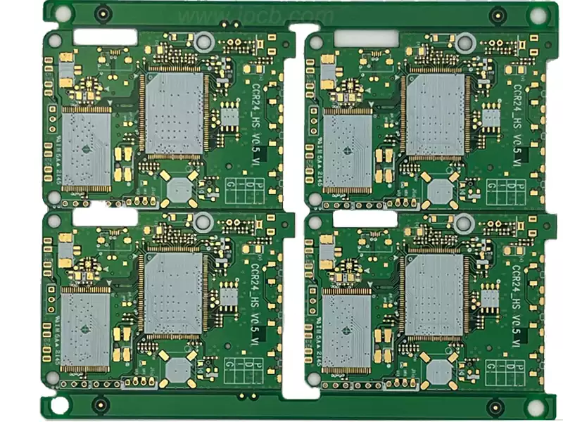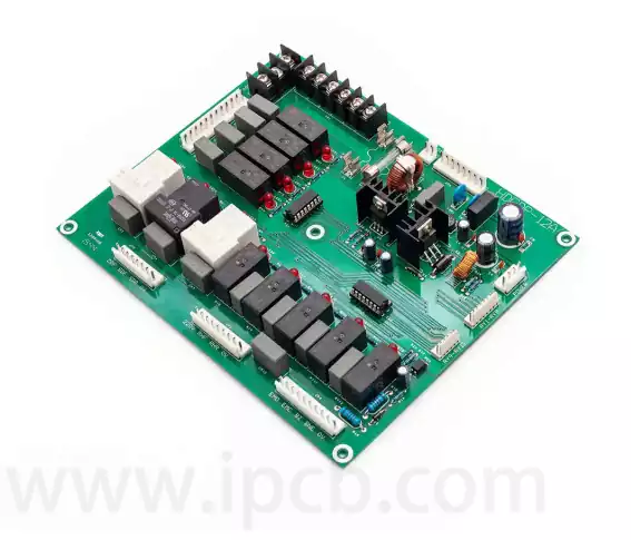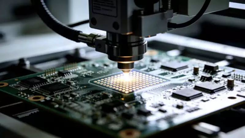
Since humanity entered the 21st century, a century intertwined with information and intelligence, every remarkable achievement of the modern electronics industry—from ultra-thin smart terminals in the palm of your hand to deep-space probes soaring through interstellar space, and massive data centers driving the global digital economy—is built upon a seemingly simple yet profoundly profound physical carrier: the Printed Circuit Board (PCB). If integrated circuit chips are the miniature brains that give devices the ability to think, then PCBs are the vast network connecting various organs, transmitting energy, and transmitting nerve signals. And in the process of transforming scattered electronic component concepts into large-scale, stably operating physical hardware, the most challenging and aesthetically pleasing step is undoubtedly printed circuit board design.
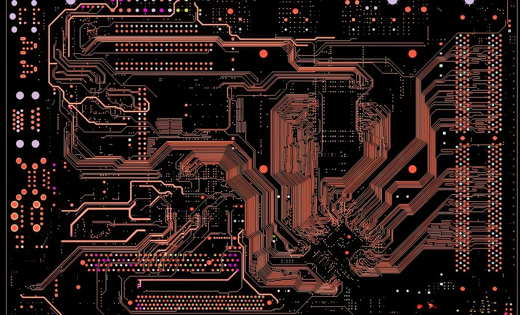
PCB-level circuit design is far more than a simple “wiring game.” It is a systems engineering project that perfectly intertwines abstract electronic schematics, complex electromagnetic field theories, polymer materials science, thermodynamic heat transfer mechanisms, and precision mechanical manufacturing processes. In the micrometer-scale spatial world and the gigahertz-scale high-frequency dynamic world, any tiny design oversight will be amplified infinitely by the laws of physics, leading to the collapse of the entire system’s performance.
From Abstract Logic to Electrical Netlist: Schematic Capture
The birth of any great circuit board begins with a seemingly chaotic yet meticulously detailed electronic schematic. This is the starting point of printed circuit board design and the first bridge for hardware engineers to translate human logical thinking into electronic flow.
Logic Mapping in Schematic Design
In the schematic capture stage, engineers use specialized Electronic Design Automation (EDA) software to modularize the circuit’s functionality. Every resistor, capacitor, transistor, complex microprocessor, or power management chip is abstracted into a graphical symbol with specific pin numbers and electrical attributes.
However, a schematic is more than just a human-readable electrical map. In modern EDA systems, each symbol is backed by rigorous electrical rules, component package libraries, material codes, and parameter attributes. When an engineer connects two wires together on the schematic, the software generates a plain text file called a “netlist” in the background. Like a master schedule in a city’s traffic network, the netlist precisely records the topological logical relationships between thousands of pins.
Electrical Rule Check and Design Pre-Approval
Before importing the abstract netlist into the physical layout design, the schematic stage must undergo an extremely rigorous Electrical Rule Check (ERC). The system automatically scans the entire schematic, looking for logical conflicts such as unconnected input pins, power outputs directly shorted to ground, or insufficient drive capability. At this stage, excellent hardware engineers must not only ensure the correctness of the circuit logic but also consider the availability of components, cost control, and the feasibility of subsequent physical layout. Every connection in the schematic lays the groundwork for the upcoming physical three-dimensional layout.
Material Selection and Physical Reconstruction of Multilayer Stack-up Architecture
Once the schematic and netlist are approved, the design work officially plunges from the two-dimensional logical world into the three-dimensional physical world. The first hurdle facing engineers is the physical skeleton design of the circuit board—material selection and stack-up architecture design.
The Physical Leap from Single/Double-Sided Boards to Multilayer Boards
In the early days of electronic technology development, circuit boards were mostly single-sided or double-sided, with all traces and components crammed onto the same plane or both sides. However, with the exponential increase in integrated circuit pin density, two-dimensional planar space was rapidly exhausted. Multilayer printed circuit board (PCB) design emerged to address this.
Modern high-performance PCBs are typically composed of dozens or even hundreds of extremely thin layers of conductive copper foil alternately laminated with insulating dielectrics. The most fundamental revolution in multilayer architecture lies in the introduction of dedicated “continuous power planes” and “continuous ground planes.” These large-area pure copper planes no longer handle sporadic signal transmission tasks but instead function as low-impedance energy reservoirs and ubiquitous electromagnetic shielding, completely reshaping the physical and electrical environment of the PCB.
Electromagnetic and Thermodynamic Properties of Core Materials The foundation of the multilayer architecture is high-performance copper-clad laminate materials. The most classic substrate is epoxy resin-glass fiber composite material (such as FR-4). When designing high-frequency, high-speed, or radio frequency circuits, the relatively high dielectric constant and dielectric loss of standard FR-4 can cause severe signal attenuation, forcing engineers to turn to high-end specialty substrates such as polytetrafluoroethylene (PTFE), hydrocarbon resins, or ceramic-filled materials.
In multilayer design, symmetry is an unshakeable ironclad rule. The lamination structure of a circuit board must be based on a physical central axis of symmetry, maintaining absolute physical symmetry from copper foil thickness and prepreg type to dielectric layer thickness. If the stack-up is asymmetrical, the circuit board will experience irreversible and severe warping during subsequent high-temperature soldering due to differences in the thermal expansion coefficients of different materials, directly causing the failure of subsequent automated surface mount technology (SMT) and mechanical assembly.
Macro-Balance and Spatial Art of Component Placement
After determining the multi-layer stack-up architecture, engineers have a blank physical canvas. The next core task is component placement. Among all circuit board design experience, there is a universally acknowledged truth: a good placement is half the battle won, while a bad placement is beyond saving.
Functional Zoning and Signal Flow Guidance
Layout is not a jigsaw puzzle of randomly stuffing components onto the circuit board, but a precise planning of spatial logic. The entire circuit board typically needs to be divided into different islands according to function: high-voltage power areas, low-voltage digital logic areas, high-frequency analog signal areas, sensitive sensor acquisition areas, and power conversion module areas.
The core principle of layout is “following the signal flow.” The main chip should be located at the core hub, surrounded by memory and peripheral interface chips that communicate with it frequently. High-frequency RF circuits must be placed close to the antenna interface; high-frequency, high-speed signals must never be allowed to traverse the entire circuit board via a long detour. By tightly clustering related components together, trace lengths can be minimized, reducing parasitic inductance and capacitance at their physical source.
Balancing Thermodynamics and Mechanical Constraints: Electronic components generate a significant amount of heat during operation. If high-power power chips or high-power MOSFETs are crammed into enclosed corners, the accumulated heat can quickly trigger over-temperature protection or even thermal breakdown. Therefore, thermodynamic management must be prioritized during the layout phase. Heat-generating devices should be kept away from thermistors and preferentially placed at edges with good airflow or in areas with reserved heat dissipation copper.
Simultaneously, layout must also compromise with the macroscopic mechanical world. The circuit board is not isolated; it must be seamlessly mounted inside a custom metal casing, plastic enclosure, or drone fuselage. The location of positioning holes, the orientation of connectors, the height limitations of large capacitors, and the ease of insertion and removal during later manual or machine maintenance are all mechanical engineering boundaries that must be repeatedly weighed during the layout phase.
Microscopic Sculpture of Routing Topology and Signal Integrity
Once the physical coordinates of components are completely locked, the core battle of circuit board design officially begins—routing. If the schematic diagram is the skeleton and the layout is the organs, then routing is the blood vessels and nerves that carry energy and information.
Transmission Line Theory and Characteristic Impedance Control
In low-frequency or DC circuits, wires are merely unobstructed channels for transmitting current. However, when the signal frequency enters the gigahertz range, and the signal edge transition time shortens to nanoseconds or even picoseconds, each printed conductor is no longer a simple conductor, but transforms into a transmission line in the form of a microstrip or stripline.
Transmission lines have distributed inductance, capacitance, and resistance characteristics, exhibiting a clear characteristic impedance. If the characteristic impedance changes abruptly along the signal transmission path (e.g., a sudden narrowing of the trace, encountering a via, or crossing a ground plane gap), high-frequency electromagnetic waves will be reflected at the point of change. This reflected wave, superimposed on the incident wave, can cause severe overshoot, undershoot, and ringing waveforms at the receiver, leading to logical errors.
To prevent signal reflection, high-end PCB designs must strictly implement impedance control. Engineers use EDA software simulations to precisely adjust the trace width, copper foil thickness, and the dielectric height of the trace from the reference ground plane, ensuring that the characteristic impedance of the entire high-speed signal line is accurately maintained at the system standard value (e.g., 50 ohms for single-ended or 100 ohms for differential).
Crosstalk Suppression and Micrometer-Level Symmetry of Differential Pairs
Within densely packed PCBs, hundreds of thousands of signal lines are arranged in parallel, inevitably resulting in electromagnetic coupling. A high-speed, rapidly changing signal line can couple noise to adjacent parallel traces through inter-line capacitance and mutual inductance—this is the troublesome crosstalk.
To suppress crosstalk, design specifications require strict adherence to the “three-times-the-line-width rule,” meaning the center-to-center distance between parallel traces should be at least three times the trace width. For buses transmitting high-speed differential signals (such as PCIe, USB, and DDR memory buses), differential pair routing is mandatory. Differential signals utilize two equally long, closely spaced wires to transmit complementary signals with opposite phases, eliminating common-mode noise introduced by subtraction at the receiving end. This requires the two differential lines to not only maintain perfect parallel spacing but also achieve absolute length matching when facing bends, controlling the phase difference between the two lines within an extremely small micrometer-level tolerance.
Protecting the Integrity of the Return Path: Current never simply goes where it wants; it must form a closed loop. For high-speed signals, the high-frequency return current doesn’t simply loop back to its source through complex power cables. Instead, it chooses the reference ground plane with the lowest impedance, directly beneath the signal line, and returns along the same path.
If a circuit board designer arbitrarily cuts huge slots into a large ground plane for ease of routing, the return current is forced to take a long detour, crossing the gap in the ground plane. This instantly creates a huge physical electromagnetic radiation loop on the circuit board, emitting strong electromagnetic interference (EMI) and severely damaging its own signal integrity. Therefore, protecting the absolute integrity of the return path is an inviolable red line in high-end wiring design.
Power Distribution Network and EMC System Defense
If signal lines are the nerves that transmit information, then the Power Distribution Network (PDN) is the circulatory system that maintains the life activities of the entire system. In a complex digital system, hundreds or thousands of transistors switch on and off simultaneously, instantly drawing huge peak currents from the power network, causing the power supply voltage to drop momentarily.
Honeycomb Array Layout of Decoupling Capacitors
To tame the high-frequency transient noise of the power network, a massive number of decoupling capacitors must be densely distributed on the circuit board.
Decoupling capacitors act as miniature local reservoirs. When a transient large current surge occurs within the chip, the local decoupling capacitors release charge within nanoseconds, filling the gap caused by the power supply voltage drop. During the design process, these capacitors must be physically positioned at the absolute forefront, closest to the chip’s power supply pins, and directly connected to the power and ground planes via extremely thick, short vias. Any excessively long leads will introduce fatal parasitic inductance, completely negating the high-frequency filtering function of the decoupling capacitors.
Electromagnetic Compatibility (EMC) and Comprehensive Shielding Matrix Modern electronic devices must pass extremely stringent electromagnetic compatibility certifications (such as FCC, CE, etc.) to prove that they neither radiate excessive electromagnetic interference to the outside world nor are immune to external electromagnetic attacks.
In the final stages of circuit board design, engineers construct a defense matrix using precise shielding and grounding techniques:
Ground mesh stitching and shielded vias: A dense row of metallized ground vias is drilled along the edges and sensitive areas of the circuit board, stitching the top and bottom ground planes together into a Faraday cage-like closed shield, locking in edge leakage of high-frequency electromagnetic waves.
Filtering and Isolation: Common-mode inductors, ferrite beads, and transient voltage suppressor diodes (TVS) are decisively deployed near all external interfaces entering and leaving the circuit board (such as power ports, network ports, and communication buses) to construct an impenetrable barrier against external lightning surges and electrostatic discharge.
Design for Manufacturing (DFM) and Delivery to the Real World
Printed circuit board design is not truly finished when all the complex schematics, multi-layer stack-ups, microwave wiring, and EMC protections are perfectly closed on the computer screen. If a drawing is flawless in the computer but cannot be manufactured with a reasonable yield on a real factory assembly line, it is still a piece of waste paper. This is the ultimate mission of Design for Manufacturing (DFM).
Accurate Export and Multi-Format Conversion of Manufacturing Data The final step in the design work is to convert complex CAD layout files into a globally recognized standard manufacturing language.
The most classic standard is the Gerber file (such as the RS-274X format), which precisely describes the geometric trajectory of the top copper layer, bottom solder mask, silkscreen characters, drill coordinates, and outline through a series of independent layer files. In recent years, the more advanced ODB++ data format has become increasingly popular. It packages all manufacturing information into a highly structured unified database, significantly reducing omissions and misalignments that may occur during file conversion.
Considerations for Solder Mask, Silkscreen, and Process Edge Design
In the microscopic view of DFM review, the size of the solder mask opening for each pad, the spacing between each character and the pad, and the tolerance of each mechanical positioning hole must all meet the limits of the PCB manufacturer’s advanced process capabilities.
For example, if the bridge width of the solder mask (green ink) is designed to be too narrow, it will break and fall off during spraying, causing bridging and short circuits between adjacent pads during soldering; conversely, if the size of the test point is smaller than the tip area of the flying probe test probe, electrical testing will be unreliable. Furthermore, to accommodate the mechanical grippers of automated surface mount technology (SMT) production lines, engineers must manually add standard “process edges” and optical positioning points (mark points) to the edges of the circuit board.
Only when these rules, which incorporate the physical limits of factory manufacturing processes, are perfectly adhered to during the design phase can the circuit board confidently fly to printed circuit board manufacturers around the world, transforming into robust and durable physical hardware.
Conclusion
Printed Circuit Board Design (PCB Design) is a rational poem spanning multiple dimensions of science. It requires designers not only to be proficient in the classical theories of electronic circuits, but also to perfectly integrate the abstract fluctuations of electromagnetic fields, the thermodynamic responses of polymer materials, and the harsh boundaries of modern automated mechanical manufacturing within the confines of a micrometer-sized world.
From the logic netlists dancing on the schematic diagram to the intricate network of impedance control transmission lines within multilayer boards; from heat dissipation in precise layouts to the final check on manufacturing yield in DFM inspections, every iteration of PCB design silently supports human society’s rapid advancement towards a future of higher computing power, wider connectivity, and ultimate reliability. A deep understanding and mastery of the underlying physics and engineering essence of PCB design is the essential path for every outstanding hardware engineer to reach the pinnacle of technology.