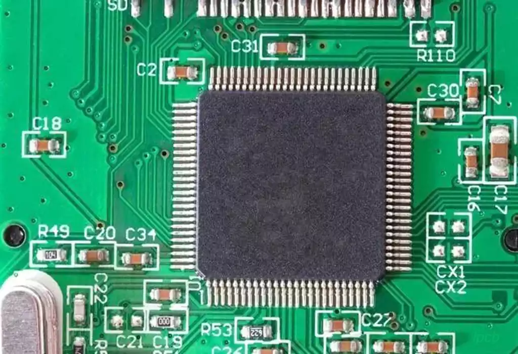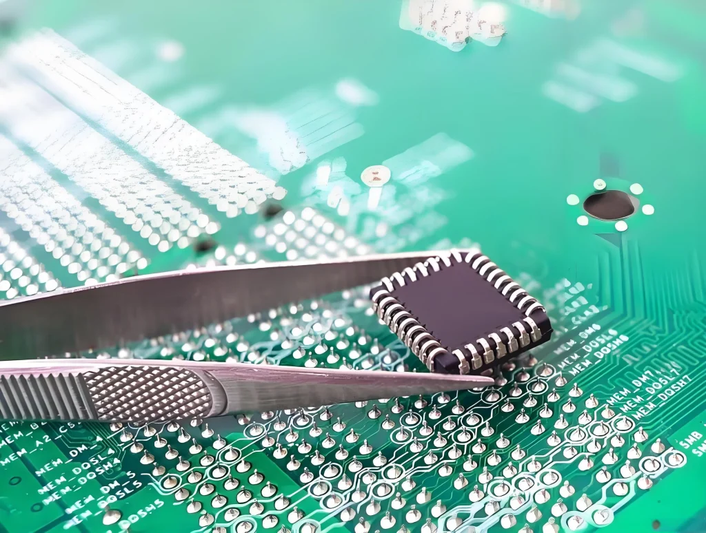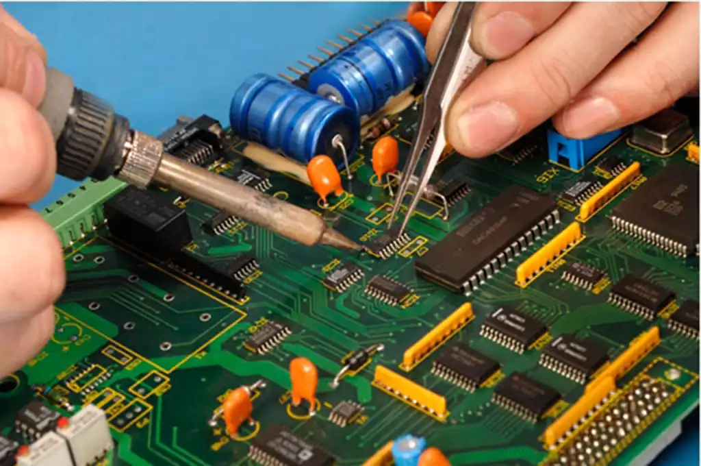
In this highly digitized information age, smart terminals, supercomputers, satellite communications, and artificial intelligence servers constitute the vast computing network of modern civilization. While we marvel at the unparalleled computing speed and exquisite functions of these electronic devices, few turn their attention to the unsung cornerstone supporting all of this—the printed circuit board laminate, commonly known in the industry as copper-clad laminate.
If we compare a complex electronic system to a towering skyscraper, then semiconductor chips are the precision electrical appliances and intelligent brain within, while the laminate is the bedrock and load-bearing reinforced concrete upon which this building rests. No high-performance circuit board can exist independently without a high-quality laminate. It not only provides robust mechanical support for tens of thousands of electronic components but also, within a micrometer-scale space, forms the core physical channel for high-speed electrical signal transmission, electromagnetic energy distribution, and heat dissipation.
A deep dive into the materials science, polymer chemical synthesis, high-pressure hot-pressing molding process, and electromagnetic thermodynamic properties of PCB laminates is essential for understanding the foundation of modern electronic hardware manufacturing.
Dissecting Copper Clad Laminates: Resin, Fiberglass, and Copper Foil
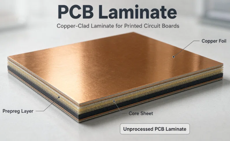
To truly understand the engineering value of laminates, one must first look beyond their glossy exterior and delve into their microscopic physical and chemical structure. A standard high-performance rigid laminate, macroscopically, appears as a flat, hard sheet, but microscopically, it is a precise “sandwich” structure composed of three distinct materials interwoven under high temperature and pressure.
Reinforcing Material: Inorganic Glass Fiber Cloth Skeleton
The core mechanical strength of a laminate comes from its internal reinforcing material. In most standard rigid laminates, this reinforcing material is a precisely woven electronic-grade alkali-free glass fiber cloth.
Glass fibers are drawn from extremely fine silica glass filaments, possessing extremely high tensile strength, extremely low mechanical deformation rate, and excellent dimensional stability. These glass fiber yarns interweave to form an inorganic skeleton within the laminate, much like a steel mesh in construction. It is the presence of this fiberglass mesh that allows the laminate to withstand welding at temperatures of hundreds of degrees Celsius, effectively restraining resin expansion and preventing catastrophic warping or cracking of the circuit board.
Matrix Material: Polymer Resin System
If fiberglass is the reinforcing steel, then the polymer resin system filling and impregnating the fiberglass mesh is the concrete.
Resin is the soul of the laminate. The most classic and widely used system is epoxy resin. During manufacturing, liquid epoxy resin needs to be thoroughly mixed with curing agents, flame retardants, and various modifying additives, then uniformly impregnated with fiberglass cloth, forming a so-called “prepreg” after a semi-curing stage. The resin not only gives the laminate excellent electrical insulation properties but also bears the crucial responsibility of firmly bonding the inorganic fiberglass cloth to the outer copper foil layer. The chemical properties of the resin directly determine the laminate’s heat resistance, chemical corrosion resistance, and long-term electrical reliability.
Functional Surface Layer: High-Purity Copper Foil
Tightly bonded to both sides of the laminate is a high-purity copper foil with precisely controllable thickness. This copper foil is typically manufactured using electrolysis, with thicknesses ranging from a few micrometers to tens of micrometers.
The copper foil forms the raw material reservoir for all conductive traces, pads, and power/ground planes on the circuit board. In subsequent printed circuit board manufacturing processes, this copper foil is precisely etched using chemical etching, transforming it into complex circuit patterns. The inner surface of the copper foil, in contact with the internal resin substrate, undergoes extremely meticulous micro-roughening treatment, forming countless nanoscale micro-anchoring points to ensure that the copper foil will never peel off from the substrate surface when subjected to intense chemical washing and high-temperature thermal shock.
Polymer Chemistry and Substrate Evolution: From General-Purpose FR-4 to High-Performance Specialty Resins
As electronic technology races towards higher frequencies, higher speeds, and higher power, traditional general-purpose laminate materials are gradually revealing their physical limitations, prompting materials scientists to continuously drive the iterative evolution of polymer chemistry.
The Classic and Universal FR-4 Resin System
In the modern electronics industry, FR-4 (Flame Retardant 4) is arguably the most dominant substrate. Here, FR stands for flame retardant, and 4 represents its material formulation level.
Classic FR-4 uses a bisphenol A type epoxy resin and dicyandiamide curing agent system, incorporating brominated flame retardants to meet fire safety standards for electronic products. FR-4 boasts excellent machinability, good electrical insulation, and a high cost-performance ratio, dominating the global market for low-to-mid-range consumer electronics, home appliance control boards, and basic industrial equipment. However, as operating frequencies reach the gigahertz level, the relatively high dielectric constant and dielectric loss of standard FR-4 have gradually become bottlenecks restricting high-speed signal transmission.
High Tg Resin and Extreme Thermal Stability
In industrial control, automotive electronics, and aerospace fields, circuit boards face extremely harsh environmental temperatures. Standard epoxy resin softens at certain temperatures, resulting in a significant decrease in its physical and mechanical properties.
To address this challenge, materials engineers have developed high Tg (glass transition temperature) laminates. By altering the resin’s crosslinking density and introducing multifunctional epoxy resins or novel curing agent systems, the glass transition temperature of high Tg materials has been increased to 170 degrees Celsius or even higher. This means that high Tg laminates can maintain extremely stable mechanical rigidity and microstructure under conditions of high-temperature exposure during lead-free soldering or continuous high-power heating, completely eliminating via fracture failure caused by resin softening.
Halogen-Free Green Laminates
Traditional FR-4 epoxy resins contain a large amount of brominated flame retardants. While these are effective at preventing fires, brominated compounds can be converted into highly toxic substances such as dioxins during the incineration of discarded electronic products, causing serious environmental pollution.
With increasingly stringent global environmental regulations, “halogen-free laminates” have emerged. Halogen-free materials completely eliminate halogen elements such as bromine and chlorine, instead employing environmentally friendly flame-retardant mechanisms such as phosphorus-based, nitrogen-based, or metal hydroxides. This not only meets the macro trend of green manufacturing but also implicitly optimizes the electrical properties and thermal decomposition temperature of resins, becoming an environmentally friendly passport for modern high-end electronic products.
High-Frequency, High-Speed Specialty Resins and Ceramic Filler Systems
When signal frequencies enter the 5G millimeter-wave, automotive millimeter-wave radar, or ultra-high-speed server bus bands, the polarization hysteresis effect of ordinary epoxy resin molecules on high-frequency alternating electric fields leads to huge energy losses.
At this point, traditional epoxy resins take a backseat, and specialty high-frequency resins, represented by polytetrafluoroethylene (PTFE), hydrocarbon resins, and polyphenylene oxide (PPO), take center stage. To further precisely control the dielectric constant and suppress thermal expansion, these specialty resin systems often uniformly mix a large amount of ultrafine nanoscale inorganic ceramic powder. These advanced laminate substrates successfully reduce the attenuation of high-frequency signals during transmission to the limit, becoming an indispensable carrier for cutting-edge communication and supercomputing hardware. Hot-press molding process: A rheological miracle under high pressure and high temperature. Transforming fiberglass cloth, resin, and copper foil into high-performance laminates is not a simple mechanical stacking process, but a high-pressure, high-temperature rheological miracle performed inside a large industrial hydraulic press.
Preparation of resin impregnation and prepreg: The first step in manufacturing begins in a precision resin impregnation workshop. Giant sheets of fiberglass cloth woven from inorganic fiberglass yarns are slowly passed under constant tension through impregnation tanks filled with a low-viscosity liquid resin solution.
After being precisely controlled by a scraper, every tiny fiber on and inside the fiberglass cloth is completely coated with liquid resin. These impregnated sheets then enter a drying oven tens of meters long. In a precisely controlled temperature field, the solvent is completely evaporated, and the resin undergoes a partial polymerization reaction, transforming from a liquid into an intermediate state with a slightly viscous surface and incomplete internal cross-linking—this is the prepreg. Prepreg is a core semi-finished raw material for multilayer circuit board lamination and double-sided laminate manufacturing.
Precision Lamination and Vacuum Environment Construction
When producing double-sided copper-clad laminates or multilayer boards, operators in a cleanroom sandwich multiple prepreg sheets between two layers of high-purity copper foil, forming a standard laminated assembly.
The symmetry of the laminated structure is crucial. If the material thickness or copper foil thickness on both sides is asymmetrical, the board will experience irreversible warping after heat curing due to uneven internal stress. The stacked “sandwich” assembly is then fed into a large multilayer hot press. Before pressing begins, the press’s internal vacuum system completely removes all air from the chamber. This step is critical; if air or even trace amounts of moisture are trapped inside the laminate, subsequent high-temperature heating will instantly vaporize it, causing bulging or delamination within the board, rendering it unusable.
Cross-linking Curing and Rheology under High Temperature and High Pressure
Once the vacuum is established, the giant hydraulic cylinders of the hot press apply immense mechanical pressure, while the heated plates rapidly raise the temperature.
Under the combined pressure and temperature, the resin, previously in a semi-cured state, melts back into a fluid. Driven by pressure, the resin, like high-quality magma, begins to flow and fill the tiny gaps in the glass fiber mesh, completely squeezing out any remaining microbubbles. Over time, the macromolecular chains within the resin undergo a complete cross-linking reaction, instantly transforming from a fluid into a robust thermosetting solid with a network structure.
The entire hot-pressing process must strictly adhere to a pre-set temperature profile and pressure gradient. Too rapid a temperature increase will result in incomplete resin curing and residual internal stress; too slow a temperature increase will cause the resin to cure prematurely before the pressure is reached, resulting in a porous interior. Only after undergoing this artful rheological refinement can a smooth, dense, and perfectly performing laminate truly be born.
Key Physical and Electromagnetic Properties: Unveiling the Core Indicators Determining Circuit Fate
On the desks of hardware engineers designing circuits, the various physical and electromagnetic parameters of laminates are crucial evidence for the successful implementation of a product. Evaluating the quality of a laminate focuses on four key dimensions.
Dielectric Constant (Dk) The dielectric constant is a physical quantity that characterizes a material’s ability to store charge under the influence of an electric field. In laminates, it directly determines the speed at which electromagnetic waves propagate through the substrate and the magnitude of parasitic capacitance between conductors.
For digital and RF engineers, the stability and value of Dk are crucial. If the dielectric constant of a laminate drifts at different operating frequencies or in different temperature environments, it will cause abrupt changes in the carefully calculated characteristic impedance of high-speed signals. Impedance mismatch can lead to severe signal reflection, waveform distortion, and increased bit error rate. Therefore, high-quality laminates must have extremely low Dk values and extremely narrow batch-to-batch variation tolerances.
Dissipation Factor (Df) The dissipation factor is an indicator of how well a laminate “stealthily absorbs” RF energy. When high-frequency alternating electromagnetic waves pass through the insulating resin, the alternating electric field drives the polymer chain segments to rub against each other at high speed, converting some valuable electromagnetic energy into useless heat energy.
A lower Df value indicates a smaller “appetite” for high-frequency signals, resulting in less signal attenuation over long distances. In today’s high-speed server backplanes and 5G communication base stations, ultra-low loss laminates are the only guarantee for perfect data delivery.
Coefficient of Thermal Expansion (CTE): Because laminates are composed of inorganic glass fibers and organic resins, their expansion behaviors under temperature changes have inherent physical differences.
Especially along the thickness direction (Z-axis), the rate of thermal expansion of resin is much greater than that of metallic copper. If the Z-axis expansion is too rapid at the high temperatures of reflow soldering, it will exert devastating longitudinal tensile stress on the plate-mounted vias (PTHs) penetrating the circuit board, causing the copper walls of the vias to break. Therefore, excellent laminates must have an extremely low Z-axis coefficient of thermal expansion to ensure the three-dimensional interconnect lifespan of high-reliability multilayer boards.
Water Absorption and Chemical Resistance
If the molecular structure of the insulating substrate contains too many hydrophilic groups, it will absorb moisture from the humid atmosphere like a sponge. Pure water has a dielectric constant as high as 80, far exceeding that of the resin substrate. Once the laminate becomes damp, its overall electromagnetic properties will deteriorate instantly.
Furthermore, water absorption weakens the interfacial bonding between the resin and glass fiber. During high-temperature welding, the enormous vapor pressure generated by moisture vaporization can directly tear and delaminate the interior of the laminate. Therefore, extremely low water absorption is the gold standard for measuring the laminate’s resistance to harsh environmental corrosion.
Interface Engineering and Copper Foil Anchoring: The Game Between Nanoscale Roughness and Bonding Force
In the manufacturing ecosystem of laminates, the bonding interface between the resin substrate and the surface copper foil is the most vulnerable point in the entire structure, most susceptible to physical and chemical challenges.
Copper Foil Surface Treatment and Microscopic Burrs
To ensure that the mirror-smooth electrolytic copper foil is firmly locked onto the epoxy resin surface, copper foil manufacturers perform complex electrochemical treatments on its inner surface.
Under a microscope, the treated copper foil surface is covered with a layer of “burrs” or “copper teeth” composed of tiny copper crystals. These nanoscale microstructures resemble countless tiny barbs. When the prepreg melts during thermopressing, the resin penetrates 100% into the gaps between these barbs, forming a strong physical-mechanical anchoring force after curing. This peel strength ensures that the circuit board will never experience copper foil detachment even after repeated severe thermal shocks and mechanical stresses.
High-Frequency Skin Effect and the Low-Roughness Revolution
However, this traditional micro-mechanical anchoring encounters a dramatic physical conflict in the high-speed, high-frequency domain.
As signal frequencies reach tens of gigahertz, the remarkable “skin effect” begins to dominate the electromagnetic behavior of the conductor. High-frequency current no longer flows uniformly across the entire cross-section of the copper foil, but rather flows in an extremely concentrated manner, tightly adhering to an extremely thin layer of micrometer-sized space on the surface of the copper foil. If the microscopic copper teeth on the surface of the copper foil are too rough, the high-frequency current is forced to undulate between these “mountain peaks,” resulting in a significant increase in the actual transmission path, a surge in conductor resistance, and severe insertion loss.
To resolve this contradiction, modern high-end laminate manufacturing has spurred the combination of “ultra-low profile copper foil” and novel chemical bonding technologies. Engineers no longer rely on crude physical mechanical “barbs” to grip the copper foil; instead, they use advanced surface silane coupling agents and chemical molecular bonding techniques to establish molecular-level chemical covalent bonds between the relatively smooth mirror-finish copper foil and the resin. This significantly reduces high-frequency conductor losses while maintaining astonishing peel strength, perfectly embodying the ultimate pursuit of extreme performance in materials engineering.
Conclusion
Printed Circuit Board Laminates are far more than just ordinary insulating plastic boards. They are the culmination of a high-level integration of modern polymer chemistry, inorganic materials science, thermodynamics, and precision fluid mechanics.
From the precise weaving of the base fiberglass cloth to the high-pressure hot-pressing rheology of high-Tg resin, from controlling the dielectric constant at every micrometer level to innovating the nanoscale interface bonding between copper foil and substrate, each revolution in laminate materials science has silently propelled the boundaries of human computing power and communication civilization ever further outward. A deep understanding of the underlying physics and manufacturing logic of laminates is not only the key to understanding the core of the entire electronics manufacturing industry, but also an excellent window to appreciate the exquisite beauty of modern industrial civilization in the micron world.