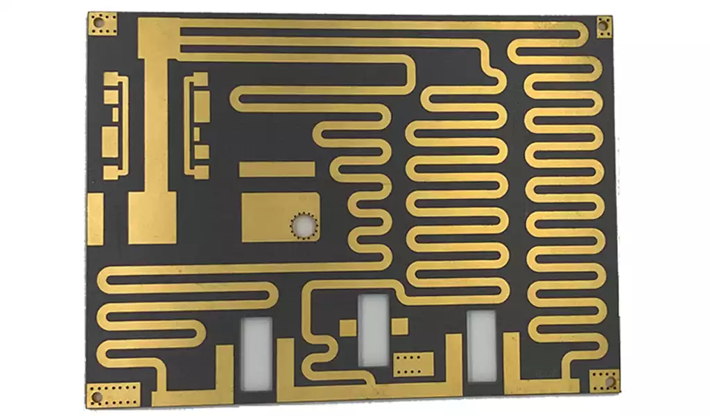
ENIG plating is a surface treatment process of Electroless Nickel/Immersion Gold. It chemically replaces palladium on the surface of copper and chemically plates a nickel-phosphorus alloy layer on top of the palladium core, and then plates a layer of gold on the surface of nickel through the replacement reaction. In short, ENIG plating is the process of forming a thin, uniform nickel-gold alloy layer on the surface of a PCB to improve its electrical conductivity, solderability, and corrosion resistance.
A comparison of ENIG Plating with other surface treatment processes is as follows:
Immersion tin (ENIG, Electroless Nickel Immersion Gold): not easy to oxidize, can be stored for a long time, the surface is flat, suitable for soldering fine-gap pins and solder joints smaller components, can withstand multiple reflow soldering, suitable for rework, and suitable for use as a COB (Chip On Board) to beat the line of the base material. However, it is more expensive, has poor solder strength, is prone to black disk problems, and the nickel layer will gradually oxidize over time, resulting in poor long-term reliability.
Sinking silver (Electroless Silver): has good conductivity and solderability, and can be applied to high-density, fine-pitch pins and solder joints. However, it is more expensive and has some pollution to the environment.
Chemical plating nickel/palladium/gold (ENEPIG): a very wide range of applications, can effectively prevent the black disk (Black Pad) defects caused by the connection reliability problems. However, the process is complex and requires strict control of process parameters to achieve the desired results.
Spray tin (Hot Air Solder Leveling, HASL): lower cost, good solderability, suitable for mass production. However, it has certain pollution to the environment and is prone to problems such as solder beads and spattering during the soldering process.
Electroless Copper (Electroless Copper): good conductivity and solderability, suitable for high-density, fine-pitch pins and solder joints. However, its cost is high and has a certain degree of pollution to the environment.
Characteristics of the immersion tin process for circuit boards
Baked at 155 ℃ for 4 hours (i.e., equivalent to storage for one year), or after 8 days of high temperature and high humidity test (45 ℃, 93% relative humidity), or after three reflow soldering still has excellent solderability.
Sinking tin layer is smooth, flat, dense, than electroplated tin is difficult to form copper-tin metal intermetallic compounds, tin-free shall.
The thickness of the immersed tin layer can reach 0.8um-1.2um, and can withstand multiple lead-free soldering impacts.
Stable solution, simple process, can be supplemented by analysis and continuous use, without changing the cylinder.
It is suitable for both vertical and horizontal processes.
The difference between immersion gold pcb and gold-plated pcb:
1.Generally immersed gold for the thickness of the gold is much thicker than gold-plated, immersed gold will be gold-colored more yellow than gold-plated, look at the surface of the customer is more satisfied with the immersed gold. The two formed by the crystal structure is not the same.
2.Due to the formation of immersed gold and gold-plated crystal structure is not the same, immersed gold is easier to weld than gold-plated, will not cause bad welding, causing customer complaints. At the same time is also because of the immersion of gold than gold-plated soft, so the gold finger board is generally selected gold-plated, hard gold wear-resistant.
3.Immersed gold plate only pads on the nickel gold, skin effect in the signal transmission is in the copper layer will not have an impact on the signal.
4.Immersed gold crystal structure is more dense than gold-plated, not easy to produce oxidation.
5.With the wiring more and more dense, line width, spacing has reached 3-4 MIL. gold-plated is prone to short-circuit gold wire. Immersion gold plate only pads on the nickel gold, so it will not produce a gold short circuit.
6.Immersed gold plate only pads on the nickel gold, so the line of solder resistors and the combination of copper layer is more solid. Engineering in the compensation will not have an impact on the pitch.
7.Generally used for relatively high requirements of the board, the flatness should be good, generally use immersed gold, immersed gold generally does not appear after the assembly of the black pad phenomenon. Sinking gold plate flatness and to be used life and gold-plated plate as good.
Reasons for choosing immersion tin surface treatment process for printed circuit boards:
Good soldering effect: immersion tin circuit board using an electroplating process, coated with a layer of tin on the surface, able to form a layer of passivated oxide layer on the board, thus protecting the copper layer, while the tin layer also plays a role in corrosion and oxidation resistance, etc., the tin and the solder joints are completely and smoothly combined together.
Improved corrosion resistance: Immersion tin circuit boards are coated with tin to protect the copper layer. The tin layer not only has the effect of reacting with common metals such as zinc, aluminum, lead and other metal oxides with corrosion and oxidation resistance but also has the property of oxidizing with the metal to form stable compounds, so the immersion tin circuit boards are more corrosion-resistant and can be used for a long time.
Affordable: The immersion tin process is simple, and low cost, but the process is more complex, but its production process is very mature, which is the immersion tin circuit board more economical and practical reasons.
Prone to short circuits: The disadvantage of immersion tin circuit boards is that the components must be spaced a certain distance apart, otherwise short circuits are likely to occur. Also, immersion tin is not suitable for the platen assembly method, because this assembly method puts a lot of pressure on the immersion tin layer. However, the assemblies on the market nowadays are using SMD assemblies, and the problem is not serious.
Not suitable for high-speed circuits: Immersion tin circuit boards are not suitable for high-speed circuits because the immersion tin in the board tends to generate reflected waves, which can have a large impact on the signal transmission speed of high-speed circuits.
ENIG plating, as an advanced surface treatment technology, has a wide range of applications in PCB manufacturing.