PCB trace impedance refers to the total resistance encountered by electrical signals during transmission across a PCB board. In layman’s terms, it represents the ‘resistance’ encountered by electrical signals as they traverse the PCB. PCB trace impedance matching denotes the adjustment and alignment of trace impedance to ensure more stable and reliable signal transmission across the PCB board.
Factors Influencing PCB Trace Impedance
Achieving impedance matching necessitates consideration not only of the PCB board’s inherent characteristics but also external factors affecting it. Key considerations include:
- Trace Width and Spacing: Trace width and spacing are primary determinants of trace impedance. Generally, narrower traces with reduced spacing result in higher impedance.
- PCB Material: The dielectric constant of the PCB material is another significant factor affecting trace impedance; a higher dielectric constant results in greater trace impedance.
- Pad and Pin Shape: The shape of pads and pins also influences trace impedance magnitude. Generally, smaller pads and pins lead to higher trace impedance.
- Signal Frequency: Signal frequency also impacts PCB trace impedance. Typically, higher signal frequencies result in higher trace impedance.
When is impedance matching required for PCB traces?
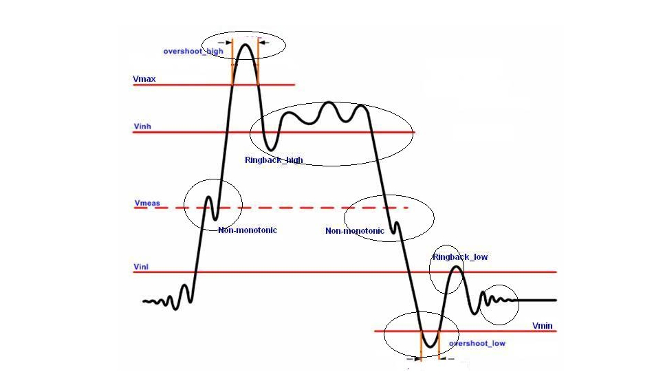
The primary consideration is not frequency, but rather the steepness of the signal edge, specifically the signal rise/fall time. Generally, if the rise/fall time (measured from 10% to 90%) is less than six times the trace delay, the signal is considered high-speed, necessitating attention to impedance matching. Trace delay is typically taken as 150 ps/inch.

In PCB design, accurately assessing trace voltage drop is crucial for ensuring stable circuit operation and performance. Below are detailed steps and considerations for calculating PCB trace voltage drop:
1.Determine Initial Parameters
Copper resistivity (ρ): First, establish the resistivity of the copper material used. Typically, this value ranges between 1.65×10^(-8) Ω·m and 2×10^(-8) Ω·m.
Trace dimensions (width and length): Measure the width and length of the PCB trace. Trace width is typically specified in mils, where 1 mil equals 0.0254 millimetres. Trace length refers to the total distance travelled by the current.
Copper foil thickness (H): Specify the thickness of the copper foil on the PCB. For example, 1 ounce (oz) copper thickness is approximately equivalent to 35 micrometres (μm).
2.Calculating Trace Cross-sectional Area
Cross-sectional area (S): Calculate the trace cross-sectional area using the formula: S = trace width × copper thickness. When performing calculations, ensure all units are converted to metres (m) for both trace width and copper thickness to guarantee accuracy.
3.Calculate trace resistance
Resistance (R): Employ a modified form of Ohm’s Law to calculate trace resistance based on copper resistivity, trace length, and cross-sectional area. The formula is: R = ρ × L / S, where L represents trace length and S denotes cross-sectional area. Ensure trace length L is also converted to metres (m), with the calculated resistance expressed in ohms (Ω).
4.Calculate Actual Voltage Drop
Voltage Drop (ΔV): Multiply the calculated trace resistance by the actual current (I) flowing through the trace to obtain the voltage drop. The formula is: ΔV = I × R, where current I is measured in amperes (A). This voltage drop ΔV represents the voltage loss incurred during current transmission along the PCB trace.
5.Consider temperature rise effects
Resistivity varies with temperature: Copper’s resistivity increases as temperature rises. This occurs because heightened thermal vibration of positive ions within the metal impedes the movement of free electrons, thereby increasing resistance. Copper’s resistivity typically rises by approximately 0.004% (40 ppm/°C) per degree Celsius increase.
Increased voltage drop: Consequently, temperature rise increases trace resistance, thereby amplifying voltage drop. In practical design, particularly for high-current applications, the impact of temperature rise on resistance and voltage drop must be accounted for.
6.Considerations for Current Density
Avoiding Overheating: Current density is a critical factor in high-current applications, as excessive current density may cause trace overheating.
Current Density (J): Current density can be calculated using the formula: (J) = I/A, where I is the current and A is the cross-sectional area of the conductor. Properly controlling current density helps prevent localised overheating and degradation of PCB performance.
7.Adjustments and Optimisation in Practical Applications
Adjusting Trace Width: During the actual design process, it may be necessary to adjust the width of traces based on specific voltage drop and temperature rise requirements.
Tool-Assisted Calculations: To enhance computational accuracy and efficiency, utilising online calculators or specialised PCB design software is recommended for detailed calculations and simulations.
8.Adherence to Design Specifications
Industry Standards: Throughout the design process, strict compliance with relevant PCB design specifications is essential, including requirements for trace width, current-carrying capacity, and voltage drop limitations.
9.Testing and Verification
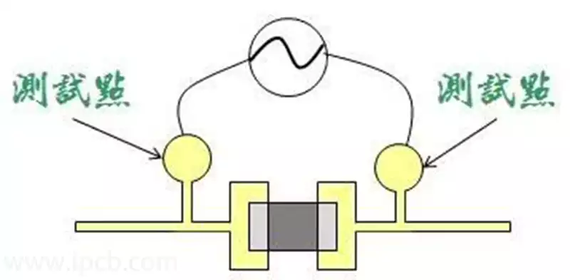
Actual Measurement: Following PCB design completion, validate whether voltage drops remain within acceptable ranges through practical testing and measurement. This confirms design compliance with performance and reliability requirements.
In PCB design, precise impedance control and voltage drop management form the cornerstone of achieving high-performance, reliable electronic products. Through systematic analysis, meticulous calculations, and rigorous testing and validation, we can effectively mitigate potential issues, ensuring stable and efficient circuit board operation.