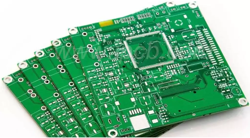
During PCB circuit boards manufacturing, copper peeling represents a relatively common issue that significantly impacts product quality. This phenomenon refers to the separation of copper foil from the substrate on a printed circuit board, potentially causing faults such as open circuits and interrupted signal transmission. Consequently, it compromises the performance and reliability of the entire electronic product.
Common causes of copper foil delamination in PCB circuit boards:
Process factors within PCB manufacturing facilities
Factors related to copper foil etching
In PCB production, the electrolytic copper foils commonly used in the market are categorised into single-sided zinc-plated (grey foil) and single-sided copper-plated (red foil) types. Typically, copper pull-off occurs predominantly on zinc-clad copper foils of 70μm thickness or greater. Red-clad foils and grey-clad foils below 18μm rarely exhibit batch-level copper pull-off issues.
Mismatch Between Etching Parameters and Copper Foil Specifications
When circuit designs progress to the over-etching stage, altering the copper foil specification without adjusting etching parameters causes excessive dwell time in the etchant. As zinc is a highly reactive metal, prolonged immersion of copper traces on LED advertising screen PCB circuit boards in the etchant causes excessive side etching. This fully reacts the zinc layer backing fine traces, detaching the copper from the substrate and resulting in copper loss.
Inadequate Post-Etching Treatment
Even with correctly configured PCB etching parameters, substandard post-etching rinsing and drying processes can trigger copper lift issues. In such cases, copper traces become encircled by residual etchant on the PCB surface. Prolonged exposure without treatment allows excessive side etching of the copper traces, ultimately causing copper lift. Such defects typically concentrate in fine-line areas. During humid weather, similar defects may appear across entire PCBs. Peeling back the copper reveals altered colouration at the substrate interface (the roughened surface), exposing the underlying copper’s natural hue. However, peel strength remains normal at coarse-line locations.
Localised Impact Factors
During LED advertising screen PCB circuit board production, localised impacts may cause copper traces to detach from the substrate due to external mechanical stress. This defect exhibits localised or directional characteristics, with detached traces showing distinct distortion or parallel scratches/impact marks. Upon peeling back the copper foil at the defective area and inspecting its surface, the copper foil’s surface colour appears normal with no signs of side etching defects, and the copper foil peel strength remains within normal parameters.
Circuit Design Factors
Unsuitable circuit design for LED advertising screen PCB circuit boards, such as employing thick copper foil for excessively fine traces, can similarly cause over-etching of the circuit lines, subsequently triggering copper pull-off issues.
Laminate Manufacturing Process Causes
Under normal conditions, provided the hot press stage of the laminate exceeds 30 minutes, the copper foil and prepreg achieve near-complete bonding. Thus, the pressing process generally does not affect the adhesion between the copper foil and substrate within the laminate. However, during laminate stacking and handling, polypropylene contamination or damage to the copper foil’s rough surface may compromise adhesion post-lamination. This can result in positioning issues (primarily affecting large panels) or isolated copper trace detachment, though peel strength tests near the affected area may show no abnormalities.
Causes related to laminate raw materials
- As mentioned in the LED advertising screen section, standard electrolytic copper foil is typically zinc-plated or copper-plated rough foil. If the rough foil exhibits abnormal peak values during production, or if the zinc/ copper plating processes exhibit poor dendritic growth, the foil’s inherent peel strength is inherently insufficient. When such defective foil is laminated into PCB circuit board stock and subsequently subjected to mechanical stress during component insertion at electronics factories, the copper traces may detach under external impact. In such cases of poor copper adhesion, examining the copper foil surface (i.e., the substrate contact face) after peeling reveals no obvious lateral corrosion, yet the overall peel strength of the foil is significantly compromised.
- Incompatibility between copper foil and resin in LED advertising screens: Certain specialised laminates, such as HTg substrates, employ distinct resin systems typically utilising PN resins. These resins feature simpler molecular chain structures and exhibit lower cross-linking during curing, necessitating copper foil with specific peak values for compatibility. When producing laminates with mismatched copper foil and resin systems, insufficient peel strength occurs during foil lamination, leading to poor copper wire retention during component insertion.
How to Address Copper Peeling on PCB Circuit Boards?
① Appropriate Material Selection
Select suitable PCB materials and adhesives, ensuring they possess adequate adhesion and thermal stability.
② Enhancing Adhesion
Employ appropriate processing methods during manufacturing, such as surface treatment and preheating, to improve adhesion between copper foil and the substrate.
③ Minimising Mechanical Stress
Employ suitable design and assembly methods during assembly and usage to reduce mechanical stress on the PCB circuit boards.
④ Strengthening Process Control
Strictly regulate temperature, humidity, and other process parameters during PCB manufacturing to ensure process stability.
⑤ Managing Thermal Expansion
Account for the PCB’s thermal expansion characteristics during the design phase to avoid excessive temperature variations.
⑥ Employ Reinforcing Materials
For areas susceptible to mechanical stress, consider using reinforcing materials or adding mechanical supports to fortify the copper foil layer.
The causes of copper pull-off in PCB circuit boards are complex, but with precise measures implemented across multiple dimensions—including materials, processes, and design—the issue can be effectively resolved. This safeguards PCB circuit boards quality and supports the steady advancement of the electronics industry.