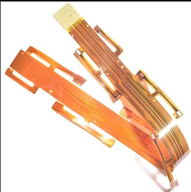
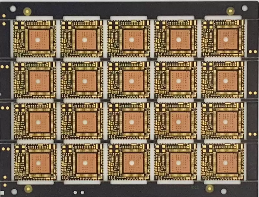
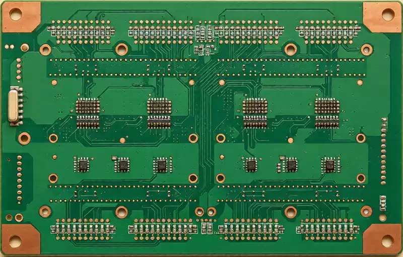
What is the bend radius of a flexible circuit board? The bending radius of a Flexible Printed Circuit Board (FPC) refers to the fact that when the FPC is bent, the two sides of its centre line are subjected to different types of stress, pressure on the inside and tension on the outside. The magnitude of the stress is related to the thickness and bending radius of the FPC, and excessive stress can lead to problems such as delamination of the FPC and copper foil breakage.
There is a limit to the bending radius of flexible PCB boards. The main feature of flexible PCB boards is that they can be bent, but due to the characteristics of the wires, electronic components and other assemblies on the board, as well as the characteristics of the material, the bending radius of flexible PCB boards needs to be limited to a certain range.
Factors affecting the minimum bending radius of flexible circuit boards:.
Flexible PCB multilayer circuit boards use flexible substrates, usually plastic materials such as polyester or polyimide. These materials have good flexibility and bending properties, but there are certain bending limits. Generally speaking, the bending radius of the flexible PCB should not be less than 20 times the thickness of the substrate. For example, if the thickness of the substrate of the flexible PCB is 0.2mm, the bending radius should not be less than 4mm.
Secondly, the bending radius of the flexible PCB multilayer circuit board should also take into account the impact of buried devices and interlayer connection. In the multilayer structure of the flexible PCB, usually embedded in some electronic devices, such as chips, resistors, capacitors and so on. These devices require sufficient space and tolerance during bending to avoid damage or failure. Therefore, the minimum radius requirement of these devices needs to be considered when determining the bending radius.
Finally, the bending radius of the flexible PCB multilayer circuit board will also be limited by the design structure. For example, if there are too many layers on the flexible PCB, or if the design configuration is not reasonable, it may lead to excessive stress and damage to the circuit board after bending. Therefore, in the design of flexible PCB multilayer circuit boards, we need to consider the reasonable control of the number of layers and the optimal design of the wiring to ensure that the requirements of the bending radius is met.
When the FPC flexible circuit board is bent, the type of pressure on both sides of the core is different. The inside of the bending surface is stressed and the outside is stretched. The amount of stress applied is related to the thickness and bending radius of the FPC flexible circuit board. Excessive pressure can cause lamination of the FPC flexible circuit board, copper foil breakage, etc. Therefore, the laminate structure of the FPC flexible circuit board should be reasonably arranged in the design, so that the curved surface of the centre line at both ends is as symmetrical as possible. At the same time, the minimum bending radius should be calculated according to different applications.
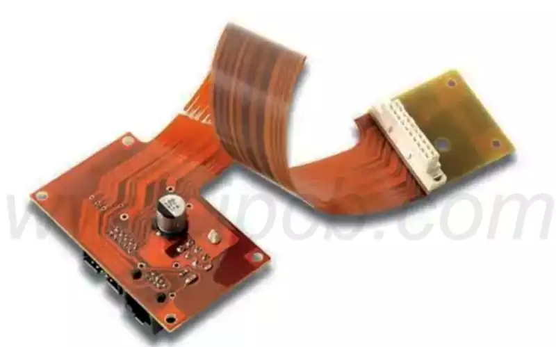
How to Calculate the Minimum Bend Radius of a Flexible PCB
Application 1. Minimum Bending of Single Sided Flexible PCBs
Its minimum bending radius can be calculated by the following formula: R= (c/2) [(100-Eb) /Eb]-D Note: R=minimum bending radius, c=thickness of the copper skin in m, D=thickness of the overlay film in m, and EB=permissible deformation of the copper skin in percentage. The deformation of copper skin varies with different types of copper.
A. The maximum deformation of calendered copper is less than 16%.
B. The maximum deformation of electrolytic copper is less than 11%.
In addition, the value of copper deformation for the same material is taken differently for different usage occasions. For one-time bending applications, the limiting value of the critical state of fracture is used (for calendered copper, the value is 16%). For bending installation designs, the minimum deformation values specified in IPC-MF-150 are used (for calendered copper, the value is 10%).
Dynamic flexibility: The application scenarios for this copper skin are realised by deformation.For example, the phosphor bronze shrapnel in an IC card is the part of the IC card that comes into contact with the chip after insertion. During the insertion process, the shrapnel will continuously deform. This application scenario is flexible and dynamic.
Application Scenario 2: Double-sided flexible circuit boards
Where: R=minimum bending radius (in m), c=copper skin thickness (in m), D=cover film thickness (in m), EB=copper skin deformation measured in percentage.
The value of EB is the same as above.
D = thickness of interlayer medium in M.
In different applications, the copper deformation takes different values, and the minimum bending radius of the FPC flexible circuit board should be calculated according to different applications.
The bending radius of a flexible PCB is a key factor that requires careful consideration. It is not only limited by the physical characteristics of the flexible substrate, but also need to take into account the ability to withstand the electronic components on the board and the overall rationality of the design. If the bending radius is not properly designed, it may lead to board damage or performance degradation.
Therefore, in determining the bending radius of the flexible PCB board, we must take into account the material properties, component layout and the use of the scene, through accurate calculations and reasonable design, to ensure that the circuit board in the process of bending not only to maintain its flexibility, but also to ensure stability and reliability.
