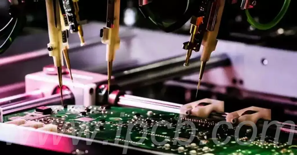
Flying probe testing is a method of testing electronic circuits, primarily for testing printed circuit boards (PCBs). It utilizes a system of movable probes that actually “fly” across the board, making electrical contact with specific test points on the PCB. Ultimately, it identifies defects and verifies the electrical performance of the circuit. A flying probe test system consists of several key components, including the probe itself, the test fixture that holds the PCB in place, and the control software that manages the test process.
Flying probe testing is also known as fixtureless ICT because, unlike traditional ICT, FPT does not require fixtures for testing. Similarly, functional testing verifies the overall performance of the assembled board. By combining these two test methods, Flying Probe Test systems provide comprehensive evaluation and valuable insights at all stages of the PCB design process to ensure the quality and reliability of specifications and performance criteria.
The basic principle of flying probe test is to place the PCB board firmly on the test bench, and then use two to four probes to move quickly and continuously between the pads and the conduction holes, in order to verify that each circuit path is consistent with the original design, or the existence of broken circuits, shorts and other anomalies. Because of the high-speed movement of the probe, the technique is called “flying probe test”. This is a basic means of electronic test verification, the advantage is that there is no need to customize a special fixture, simply fix the board in the device (whether up and down or left and right directions), very suitable for small batch or sample testing; however, the shortcomings of the test is that the test time is longer, especially when the number of points to be tested increases, the time consumed will be even longer, and therefore is not suitable for large-scale mass production of the board’s test.
The goal of flying probe testing:
Defect detection: Flying needles testing has the ability to quickly identify all types of defects in the PCB manufacturing process, such as shorts, breaks and positional deviations. This process not only confirms the existence of defects, but also pinpoints their location, laying a solid foundation for subsequent repair operations.
Performance Verification: In addition,flying probe testing is responsible for verifying the electrical performance of PCBs to ensure that they conform to design and production specifications. By comprehensively examining core indicators such as signal integrity, impedance values and current paths,flying needles testing ensures that products perform well in real-world application scenarios, effectively reducing the incidence of failures.
Production Optimization: With continuous test feedback, flying needles testing helps manufacturers identify potential hazards in the production process, optimize the production process, and improve overall production efficiency.
Quality Assurance: In a competitive market environment, product reliability has become the key to victory.Flying probe test provides strict quality control for each PCB to ensure that it meets industry specifications and customer expectations, which protects the competitiveness of products in the market.
Flying probe test process:
Test data preparation:
This step generates production data based on customer originals to ensure that no test points are missed during the test process that may be caused by inconsistencies between the production and original drafts.
Execute the test:
The flying probe test utilizes a single needle to contact the test pads or test points one by one to perform a thorough inspection of the line network.The length of the test depends on the complexity of the network and the number of test points. The attached figure shows an example of a flying needles tester and its working condition.
Result Determination and Repair:
For locations that fail (NG) the test, confirm and repair based on the network diagram, and scrap those that cannot be repaired.
Fixture testing process:
Fixture production:
The test fixtures are designed for mass production and are made according to customer’s original drawings. The production process is more complex, the cost varies according to the complexity of the network, the number of test points, the size of the test pad and other factors. Once the fixture is made, it can be reused within a specific lifetime, and should be stored in a moisture-proof manner to prevent oxidation of the test pins and components.
Testing:
Use a special test machine for testing, test racks need to be installed before testing and debugging and first board inspection. After passing the first board inspection, mass production can be carried out. The attached figure shows the working status of the automatic test machine during the test, the red box is the test frame.
Result determination and repair:
Judge the non-conforming goods (NG) tested and repair or scrap them.
In the testing process, in addition to paying attention to the open and short-circuit problems of the product itself, it is also necessary to pay attention to whether the pads appear to be crushed during the testing process and other appearance problems.Especially when using the test rack for testing, in addition to the first and last pieces of inspection, but also need to carry out random testing to ensure product quality.
As an efficient and flexible electronic circuit test method, flying probe test plays a pivotal role in the PCB manufacturing and verification process. It not only accurately detects manufacturing defects and verifies electrical performance, but also provides strong support for production optimization and quality assurance. Although it has shown significant advantages in small batch or sample testing, its time-consuming nature still needs to be considered for large-scale mass production board testing.
