Introduction
In modern electronics manufacturing, printed circuit boards (PCBs) are considered the “heart” and “nervous system” of electronic products. From smartphones and wearables to automotive electronics, medical devices, and aerospace, the functionality of nearly all electronic products relies on PCBs. However, as PCBs accelerate toward higher density, miniaturization, and multi-layered design, quality issues are becoming more complex and insidious. Ensuring the electrical performance and structural reliability of PCBs before they enter assembly has become a key industry concern.
Traditionally, PCB inspection relies on manual visual inspection or simple electrical testing equipment. However, as circuits become increasingly complex, manual testing can no longer meet the dual requirements of high precision and efficiency: the human eye struggles to detect micron-level defects, and manual testing speeds far lag behind the pace of mass production. To address these challenges, automated PCB testing machines have emerged, representing a key step toward automated and intelligent quality control in electronics manufacturing.
An automated PCB testing machine utilizes high-speed probes, advanced sensors, and intelligent software systems to perform fast, accurate, and comprehensive testing of circuit boards. Compared to manual methods, it can:
Complete inspections of hundreds or even thousands of test points in a fraction of the time; accurately capture minute defects, eliminating human error; and digitize and store test data, providing a basis for subsequent quality analysis and process improvements.
More importantly, an automated PCB testing machine is more than just testing equipment; it is a key component of an intelligent manufacturing system. It integrates with upstream design and downstream assembly processes, achieving full-process quality traceability through a closed-loop data loop, significantly improving the reliability and competitiveness of the entire production system.
Thus, an automated PCB testing machine is more than just a tool; it represents a shift in manufacturing philosophy. It signals the electronics industry’s accelerated entry into a new era of automation, data-driven development, and intelligence. Next, we will further explore the fundamentals and significance of PCB testing to understand why testing is an essential component of PCB manufacturing.
The Fundamentals and Significance of PCB Testing
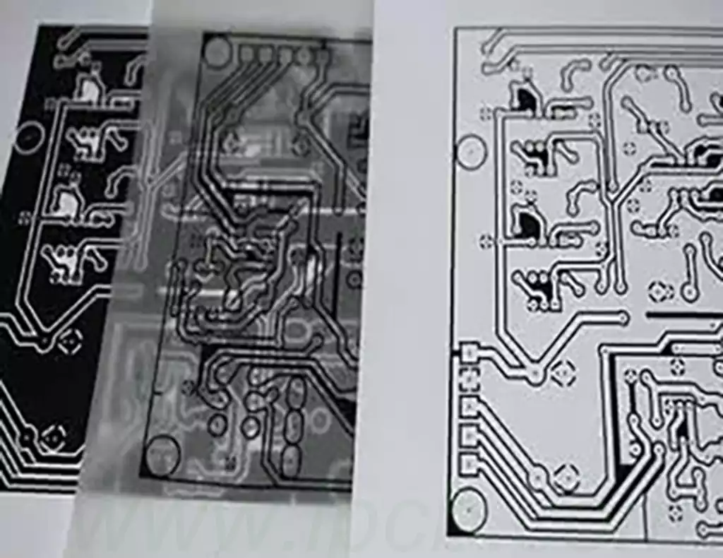
In the PCB manufacturing process, every step of design and production can harbor potential risks. The trace etching process can cause open circuits or residual copper. Drilling and plating can create rough hole walls or electrical discontinuities. Pad processing can result in offset or insufficient plating. If these defects go undetected, they can directly impact the functionality and lifespan of electronic products. Therefore, the goal of testing is to identify and eliminate potential problems as early as possible, ensuring qualified circuit boards enter assembly.
Main Items of PCB Testing
Common PCB test items include:
Continuity testing: Ensures that electrical connections between circuit networks are intact and correct, avoiding open circuits.
Short circuit detection: Identifies short circuits caused by residual copper, solder bridging, or design deviations.
Impedance control: Particularly important for high-frequency circuits, ensuring stable and consistent signal transmission.
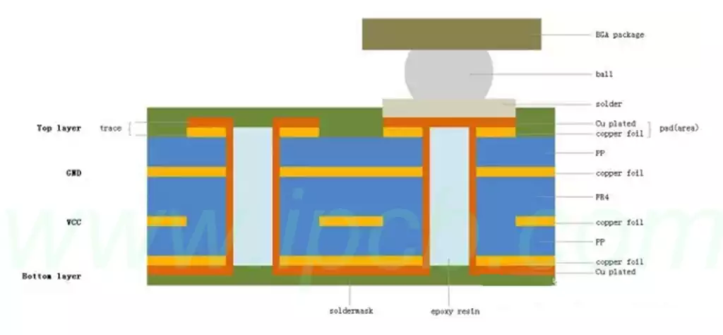
Interlayer alignment: In multi-layer PCBs, confirms that traces and vias are precisely aligned to avoid signal interference.
Pad reliability: Tests the quality and adhesion of the pad plating to ensure stability during subsequent soldering.
These tests go beyond simply screening for “pass/fail” results; they also provide feedback on manufacturing quality, helping factories improve processes and increase yield.
Limitations of Manual Testing and Early Inspection Methods
Before the widespread adoption of automated equipment, PCB testing primarily relied on manual labor and simple tools. For example, operators would observe circuit defects through a magnifying glass or perform point-to-point inspections using simple continuity testers. While these methods were acceptable for early, low-volume production, they had significant drawbacks:
Inefficiency: Manual inspection is time-consuming and labor-intensive with tens of thousands of test points.
Lack of Accuracy: The human eye has limitations in detecting micron-level defects, making them prone to missed detections.
Poor Consistency: Different inspectors use different judgment criteria, making it difficult to ensure consistent results.
Unable to Handle Complex Circuits: With the prevalence of high-density interconnect (HDI) and multilayer boards, manual methods are becoming increasingly inadequate.
The Necessity of Automated Testing
With the rapid development of the electronics industry, PCBs require not only high density and reliability but also consistent quality under large-scale production. This makes automated testing an inevitable trend:
Adapting to complex designs: Automated testers can quickly handle tens of thousands of test points with far greater accuracy than manual testing.
Improving efficiency: In mass production, the speed and stability of automated testing are critical to ensuring delivery.
Reducing costs: Although the equipment investment is high, in the long run it can significantly reduce rework and scrap, lowering overall manufacturing costs.
Enabling data-driven management and control: Test data is automatically stored and analyzed, providing strong support for process optimization and traceability.
Therefore, the introduction of automated PCB testing machines not only replaces manual testing but also upgrades quality control systems. They truly bring PCB manufacturing onto the path of Industry 4.0, achieving efficient, accurate, and intelligent testing.
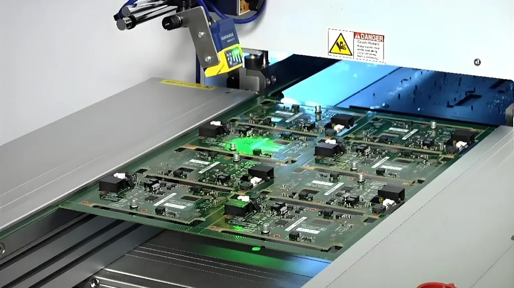
How Automated PCB Testing Machines Work
An automated PCB testing machine is a comprehensive device that combines precision mechanics, electronic circuitry, and intelligent software. Its essential task is to verify every circuit network on a PCB through efficient and accurate testing methods to ensure that its electrical performance meets design requirements. To better understand its principles, we can focus on its structure, test process, and different types.
Core Components
A typical automated PCB testing machine typically includes the following key modules:
Probe system. The probe is the key component that allows the machine to contact the PCB and complete the test. The probes in automated equipment feature high sensitivity and a long lifespan, enabling rapid switching between different test points. The probes in flying probe testers also feature high-precision positioning capabilities, allowing them to directly contact any trace or pad.
Control and drive system. This includes motors, drives, and motion platforms to achieve precise movement and positioning of the probe on the PCB. High-end equipment typically uses servo motors and linear guides to ensure a balance between speed and accuracy.
Signal acquisition and analysis module. Using a signal generator and detection circuitry, current or voltage is injected into the PCB and the response is measured. The software system analyzes whether the circuit network meets expectations and whether there are shorts, opens, or impedance anomalies.
Automation software platform. The software not only controls the machine’s operations but also manages test data, generates reports, and integrates with MES (Manufacturing Execution Systems) or ERP systems for data traceability and process optimization.
Automated Testing Process
The typical workflow of an automated PCB testing machine is as follows:
Board Loading: An operator or loading system places the PCB on the machine’s worktable. Some high-end machines support automatic loading and unloading.
Positioning and Identification: The machine uses a vision system or positioning holes to confirm the precise position of the PCB, preventing testing errors.
Probe Contact and Scanning: Flying probes or fixture probes contact the circuit network one by one according to a preset program, injecting signals and collecting responses.
Data Analysis: The system compares the design file (such as the netlist) with the actual test data in real time to identify mismatches.
Result Output: The machine automatically generates a test report showing passed and failed items and saves the data to a database for future traceability.
This process is almost fully automated, requiring only manual loading and unloading operations and minimal monitoring, significantly reducing human intervention.
Common Types of Automated Testers
Currently, common automated PCB testing machines in the industry can be categorized as follows:
Flying Probe Testers. These machines require no specialized fixtures, allowing the probes to be freely moved to any location on the PCB. This makes them suitable for small-batch, high-mix production. However, their relatively slow testing speed is a drawback.
Bed of Nails Testers. These machines use custom fixtures to contact all test points on the PCB at once, resulting in extremely fast testing speeds and suitable for large-scale mass production. However, fixtures are expensive and require re-manufacturing when changing products.
Automated Optical Inspection (AOI) combined with electrical testing. These machines use optical imaging to quickly identify surface defects and then combine with electrical testing to verify circuit performance. They are suitable for providing dual assurance of delicate traces and pads.
These types of testers are often not used in isolation, but rather flexibly combined based on production scale and product characteristics. For example, flying probe testing can be used for rapid verification during R&D, while fixture testing can improve efficiency during mass production.
Comparison and Application Scenarios of Different Testing Methods
In PCB manufacturing, automated PCB testing machines are not a single type but encompass a variety of testing technologies. Different types of automated testing machines have their own characteristics in terms of speed, cost, accuracy, and scope of application. Understanding these differences will help factories select the appropriate solution based on their needs.
Flying Probe Testing. A flying probe tester uses movable probes to contact the circuit point by point, performing electrical testing according to the netlist in the design file.
Advantages: No fixtures are required, offering high flexibility and suitable for high-mix, small-batch orders. It is highly efficient during new product development and pilot production. It can inspect small pads and high-density traces, making it suitable for complex circuit boards.
Disadvantages: Slow test speeds, making it less efficient for high-volume production. The number of probe contacts is limited, and prolonged operation can lead to wear.
Application Scenarios:
Mostly used for sample verification, small-batch orders, and the R&D phase of high-end, complex boards (such as those in the medical and military industries). Bed of Nails Testing: A bed of nails testing machine uses a customized test fixture to simultaneously press-connect thousands of probes to a PCB, enabling one-touch testing.
Advantages: Extremely fast testing speed, suitable for large-scale mass production. All test points can be inspected simultaneously, far exceeding flying probe testing. After amortizing the costs, it is very economical for long-term production.
Disadvantages: High fixture production costs and long lead times. Product changes require re-customization of the fixture. Limited compatibility with ultra-fine-pitch components or complex designs.
Application Scenarios:
Suitable for consumer electronics and large-scale production orders, especially when the same product model requires long-term stable production.
Combining Automated Optical Inspection (AOI) with Electrical Testing
AOI uses high-resolution cameras and image processing algorithms to detect PCB surface defects such as broken wires, shorts, residual copper, and pad defects. Its advantages are high speed and non-contact inspection, making it particularly suitable for high-density circuits.
When AOI is combined with electrical testing, dual assurance is achieved:
AOI performs structural and visual inspections to identify potential defects;
Electrical testing verifies functional performance, ensuring circuit functionality.
This combined approach overcomes the shortcomings of a single inspection method and provides more comprehensive quality control.
Method Comparison Summary
Flying probe testing: Highly flexible and suitable for small batches and complex boards, but slower.
Jig testing: Fastest and suitable for large-scale production, but with high fixture costs.
AOI + electrical testing: Suitable for high-precision and high-density circuits, providing more comprehensive assurance.
In practice, factories often make a comprehensive choice based on product type, order size, and lead time. For example, a mobile phone motherboard manufacturer might use flying probe testing during the R&D phase and switch to jig testing during mass production, while also using AOI to ensure both visual and electrical performance compliance.
It can be said that different testing methods are not substitutes, but rather complementary. A reasonable test combination can achieve the optimal balance between speed, cost, and quality.
As the PCB industry moves toward high precision, high density, and high reliability, the use of automated PCB testing machines has become a core component of modern manufacturing. Automated testing not only improves efficiency but also upgrades quality assurance systems. However, its benefits come with challenges.
Advantages of Automated Testing
Dramatically Improved Efficiency. Compared to manual testing, automated equipment can verify thousands of test points in a fraction of the time. For fixture testing machines, they can inspect the entire board in a single press, making their speed advantage particularly significant in high-volume production.
Precision and Consistency. Automated equipment, with its precise control and stable probe system, enables micron-level accuracy, eliminating errors caused by human judgment and ensuring consistent test results.
Adapting to Complex Circuit Designs. With the prevalence of high-density interconnect (HDI) and flexible circuit boards, circuit designs are becoming increasingly complex. Equipment like flying probe testers can flexibly handle complex networks and high-precision pads, eliminating blind spots that are difficult for humans to reach.
Dataization and Traceability. Automated equipment test results can be saved in real time and connected to the Manufacturing Execution System (MES) for data tracking and statistical analysis. This data-driven approach helps identify process bottlenecks and improve process quality.
Long-term cost optimization. Although the initial investment in automated equipment is high, it can significantly reduce overall manufacturing costs and enhance company competitiveness in the long term by improving yield, reducing rework, and reducing scrap.
Challenges of Automated Testing
High equipment investment costs. High-end automated testers can cost hundreds of thousands of dollars, a significant expense for small and medium-sized enterprises. The additional cost of fixture production further increases the cost burden for small-batch production.
Technical barriers and maintenance difficulties. Automated test equipment involves precision mechanics, electronic controls, and software platforms, requiring a specialized team for operation and maintenance. Lack of technical support can lead to underutilization of the equipment.
Balancing speed and flexibility. Flying probe testing is flexible but slow, while fixture testing is fast but less flexible. Finding the right balance between efficiency and flexibility is a crucial consideration for factories when selecting equipment.
Challenges Brought by Complex Designs
With the rise of 5G, high-speed signals, and automotive electronics, PCB requirements for impedance and signal integrity are becoming increasingly stringent. Traditional electrical testing may not be able to fully cover these requirements, necessitating the integration of more advanced testing technologies (such as X-ray, ICT, and functional testing).
Integration with Smart Manufacturing
Although automated testing generates large amounts of data, the industry is still exploring how to effectively integrate it into smart manufacturing systems to achieve closed-loop feedback and process optimization.
The Dialectical Relationship Between Advantages and Challenges
It can be said that automated testing is not a one-size-fits-all solution. While it is a powerful tool for improving PCB manufacturing quality, it also presents financial and technical challenges. Companies need to choose the right approach based on their scale, order structure, and product characteristics.
Appropriate automated testing solutions.
More importantly, automated testing shouldn’t be viewed simply as a single upgrade, but should be considered within the context of the entire smart manufacturing ecosystem. The true value of automated PCB testing machines can only be realized when a closed data loop is formed between design, production, and testing.
Future Development Trends and Industry Prospects
As electronic products evolve toward higher frequencies, higher speeds, miniaturization, and intelligent manufacturing, PCB manufacturing and testing technologies are also evolving. In the future, automated PCB testing machines will become more than just testing tools; they are likely to become core nodes in the smart manufacturing ecosystem.
Intelligent and data-driven. Future automated testing equipment will increasingly rely on artificial intelligence (AI) and big data analytics. By collecting and analyzing large amounts of test data, equipment can:
Predictive maintenance: Identify and perform maintenance before probe or circuit anomalies occur, reducing downtime.
Process optimization: Through data backtracking, identify the source of defects in the production process and drive process improvements.
Adaptive testing strategies: Automatically select the optimal testing method based on the design characteristics of different products, improving flexibility and efficiency.
Deep Integration with Smart Factories
In the context of smart manufacturing and Industry 4.0, automated PCB testing machines will no longer be isolated inspection units but will be embedded in the entire production line:
Seamless integration with MES/ERP systems enables real-time linkage between production data and test results;
Combined with robotic loading and unloading, unmanned inspection stations will be realized; and edge computing will enable rapid decision-making, improving the overall intelligence level of the production line.
High-density and high-speed PCB testing requirements
The development of 5G, automotive electronics, and medical electronics has placed higher demands on signal integrity and impedance control in PCBs. Future testers will need to feature:
Higher-precision probe control to accommodate high-density circuits with micron-level pitch;
High-speed signal testing capabilities to ensure the performance of high-frequency PCBs within the actual operating frequency band;
Flexibility to accommodate diverse substrates such as flexible circuits (FPCs) and rigid-flex boards.
Integration of Automation and Multi-Dimensional Testing
In the future, single-source electrical testing may no longer be sufficient to meet industry needs. Automated testing equipment will tend to integrate multiple functions:
Electrical testing + AOI + X-ray to achieve comprehensive coverage of appearance, soldering, and electrical performance;
ICT (in-circuit testing) combined with functional testing directly verifies the actual working state of the circuit;
Environmental simulation testing, combining temperature, humidity, and electrical stress testing, verifies the reliability of circuit boards under extreme conditions.
Global Market Outlook
According to industry forecasts, with the continued growth of automotive electronics, 5G communications, and consumer electronics, the global PCB industry will continue to maintain steady development. Correspondingly, demand for automated testing will also expand:
Asia (particularly China and Southeast Asia) remains the main manufacturing center, with the strongest demand for high-efficiency test equipment;
The European and American markets are more focused on the integration of high-end equipment with smart manufacturing;
Emerging applications such as wearable devices and smart homes will also drive demand for small-batch, diversified testing, creating more opportunities for flying probe and flexible testers.
It is foreseeable that in the future, automated PCB testing machines will not only be inspection tools, but will also become a key support for manufacturing process optimization, intelligent management, and product quality assurance. It is not only the “gatekeeper” of industry development, but also an important driving force for pushing the electronics manufacturing industry to a higher level.