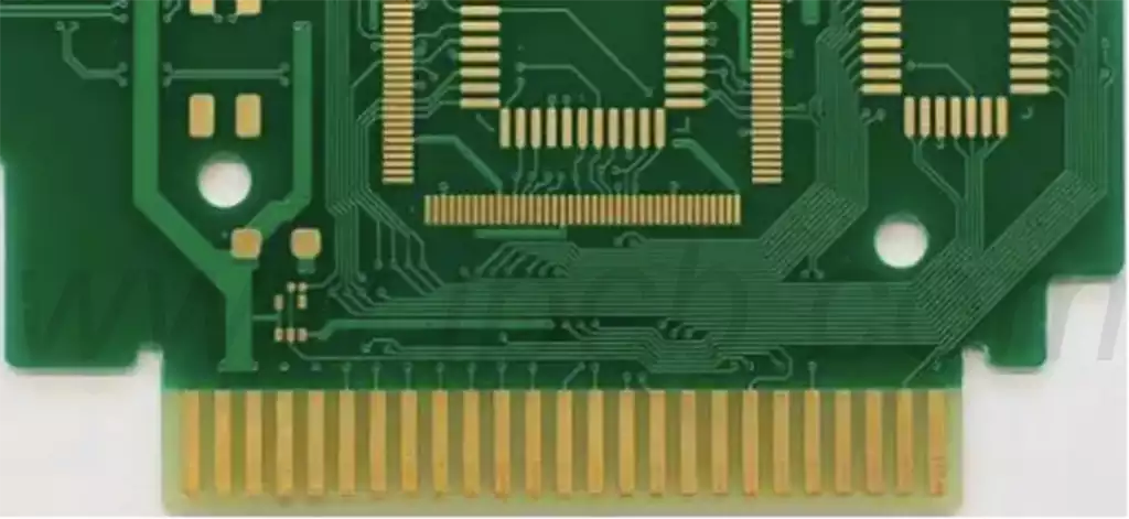
Gold finger pcb is metal connectors that are set on the edges of a circuit board and usually take on a gold or yellow appearance. These connectors are made of gold-plated or alloy materials and are designed to provide a reliable electrical connection and are commonly used to connect different electronic components such as memory sticks, graphics cards and other expansion cards to the motherboard.
The main function of gold fingers is to enable signal transmission and power connections between circuit boards. Through gold fingers, signals can be efficiently passed between the slots and the circuit boards to ensure the proper functioning of the devices. In a variety of electronic devices, such as computers and smartphones, gold fingers play an important role and enhance the overall performance.
Gold finger pcb process flow
- Design stage
In the design phase of the gold finger PCB, engineers need to pay attention to several factors, including the chamfer of the gold finger, solder resist window treatment and the distance between the gold finger and the pad. These design requirements ensure that the gold finger can be accurately inserted into the connector and avoid poor contact problems during use. - Cleaning Steps
Before plating can begin, the copper conductor surface of the PCB must be cleaned. This process is aimed at removing impurities such as dirt, grease and oxides from the surface, and is usually done by physical or chemical methods such as ultrasonic cleaning or polishing to ensure good adhesion for subsequent gold plating. - Electroplating process
After the cleaning is completed, the electroplating step can be carried out. At this stage, the PCB substrate will be immersed in a gold-containing plating solution, and metallic gold will be deposited on the surface of the gold finger to form a conductive layer. Controlling the plating time, temperature and chemical concentration is crucial for the uniformity and thickness of the gold layer.
4.Testing
After plating is completed, the conductivity and mechanical connectivity of the gold finger is tested to ensure that it meets the design requirements. Testing is key to the performance of the Gold Finger PCB, and can identify and correct problems to prevent failures in subsequent use.
- Quality Control
Finally, conduct comprehensive quality control, including appearance inspection and performance testing. Establishing strict quality standards and processes helps to improve the reliability and durability of Gold finger PCB and reduce product defect rates. These measures ensure that the final delivered products perform well in various usage environments.
Advantages:
High conductivity: Gold is a highly conductive metal, so the use of gold fingers ensures low impedance and high reliability in signal transmission.
Corrosion resistance: gold has a strong corrosion resistance, so in a variety of environments can maintain stable performance, not easily affected by oxidation or corrosion.
Good contact performance: Gold fingers can form good contact with various connectors or slots to ensure low impedance and high reliability of signal transmission and current transmission.
High reliability: Because gold finger has high conductivity, corrosion resistance and good contact performance, its reliability is very high and can ensure long-term stable use.
Disadvantages:
High manufacturing cost: Since gold is an expensive metal, the use of gold fingers increases the manufacturing cost of the circuit board.
Easy to pollute: gold fingers are easily contaminated by dust, dirt or other impurities, affecting their conductivity and contact performance.
High soldering requirements: Since gold has a high degree of thermal sensitivity, special care is needed during the soldering process to avoid damage to the gold finger.
High repair costs: If the gold finger is damaged or malfunctions, the repair costs can be very high as the entire board needs to be replaced or advanced repairs need to be made.
The problem of uneven thickness of the gold plating layer during the manufacturing process of gold finger PCB can be solved by several technical means. These include improving plating process conditions, optimizing plating time, controlling temperature and concentration, and using specialized equipment for fine control to ensure more uniform plating thickness.
- Improvement of process conditions
Improving the plating process conditions is one of the key measures to solve the problem of uneven thickness of the gold plating layer. By carefully controlling the PCB plating process parameters, such as current density and plating time, the uniformity of the gold plating layer can be effectively improved. Especially in the use of ENIG (nickel – gold) process, need to pay attention to reduce the number of gold layer pinholes and try to increase the thickness of the gold layer to ensure the surface quality. - Optimize plating time
The length of the plating time directly affects the thickness of the gold layer. Therefore, when plating gold fingers, the plating time can be adjusted to achieve a more uniform plating effect. Reasonable plating time length can make the metal deposition more uniform, thus avoiding the thickness difference. - Control temperature and concentration
The temperature and concentration of chemicals in the plating process are also important factors affecting the uniformity of the gold plating layer. Appropriately increasing the temperature of the plating solution and controlling the concentration of components in the plating solution can promote uniform deposition of metal ions and reduce the risk of uneven plating due to temperature differences. - Use of fine control equipment
The introduction of advanced production equipment, such as automated plating machines, can realize automated control of the plating process. These devices can monitor and adjust the plating conditions in real time, thus effectively reducing the fluctuations caused by human factors and ensuring the uniformity of the thickness of the gold plating layer.
5.Regular Quality Inspection
Finally, it is important that the thickness of the plating layer is checked regularly. Through the use of appropriate thickness measurement tools, such as X-ray fluorescence analyzers, the thickness of the plating layer can be found in a timely manner and adjusted accordingly to ensure that the final product even in the production batch changes still maintain stable quality.
Application Areas of Gold Finger Printed Circuit Boards
- Automotive electronics
In automotive electronics, gold finger pcb is used to connect the various components of automotive instrument panels for signal transmission and power connections. These connections ensure the proper functioning of the instrument panel and the accurate display of real-time data, thus enhancing the safety and performance of the automobile. - Computer Hardware
Gold finger pcb is also widely used in computer hardware, especially on memory sticks, graphics cards and other expansion cards. These gold fingers enable various hardware to realize high-speed data exchange and function expansion by connecting with the slots on the motherboard. - Audio system
In automotive and home audio systems,gold finger pcb is used to connect multiple components of audio equipment to enable transmission of audio signals. This design not only improves the sound quality,but also increases the stability of the system. - Industrial Automation
Gold finger PCB is also widely used in industrial automation equipment.For example, in mechanized equipment in processing plants and automotive factories, Gold finger is used to connect internal circuit cards to ensure efficient operation and real-time communication of the equipment. - Consumer Electronics
In addition to the above areas,gold fingers are also used in consumer electronics such as cell phones and tablets.These devices rely on gold fingers to realize quick connections between different components, improving overall performance and user experience.
Gold finger pcb plays an indispensable role in modern electronic devices and are widely used in computer hardware, automotive electronics, and consumer electronics due to their excellent conductivity and reliability. Despite some challenges, such as manufacturing costs and susceptibility to contamination, high-performance Goldfinger PCBs still provide stable connectivity solutions for a variety of devices. With the advancement of technology, the prospect of its application will be even broader.