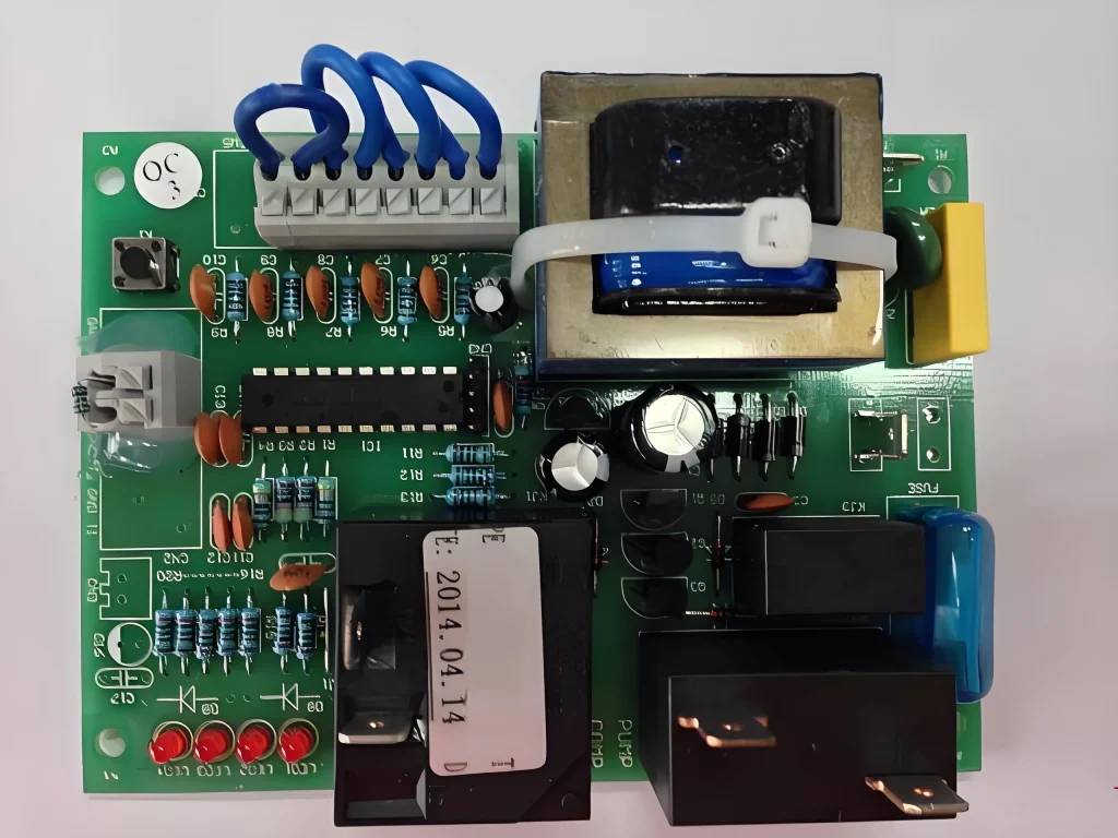
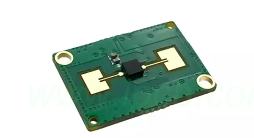
With the advancement of modern electronic technology, the trend towards high-frequency signal transmission and high-speed digitalisation has become mainstream, making high frequency PCB design a crucial field of research.
High frequency circuit boards are typically defined as boards handling electromagnetic frequencies exceeding 1GHz, imposing heightened demands on substrate properties, routing, and overall design.
In high-frequency scenarios, surface treatments primarily influence impedance through three mechanisms: Firstly, the cumulative effect of the skin effect — when the skin depth is less than the treatment layer thickness, current flows entirely through this layer. Consequently, the resistivity of the treatment layer directly determines the conductor’s equivalent resistance, thereby affecting characteristic impedance. For instance, in the gold immersion process, gold’s resistivity (2.44×10⁻⁸ Ω・m) is 1.4 times that of copper (1.72×10⁻⁸ Ω・m). At 10GHz, transmission lines using gold immersion exhibit impedance 4-5Ω higher than pure copper conductors. Secondly, the impact of surface roughness — High-frequency signals are highly sensitive to conductor surface smoothness. Rough treatment layer surfaces (such as the tin-lead layer in HASL processes) increase signal transmission loss while causing high-frequency fluctuations in impedance values. Thirdly, the dielectric loss of the treatment layer — certain surface treatment layers (such as OSP) possess a dielectric loss tangent, absorbing signal energy at high frequencies and indirectly altering impedance characteristics.
In practical calculations, engineers must employ impedance models specifically designed for high frequencies. For instance, traditional microstrip impedance formulas (such as Wheeler’s formula) neglect the coupled effects of skin effect and surface treatment, yielding significant errors at high frequencies. In such cases, three-dimensional models based on electromagnetic simulation must be adopted, incorporating the microstructure of the treatment layer (e.g., roughness, thickness distribution) into the simulation. Taking a 5G RF PCB design as an example, employing a silver-plated process (silver layer thickness 3μm), the impedance value calculated using a three-dimensional simulation model at the 28GHz frequency band was 49.8Ω. This yielded an error of only 0.6% compared to the actual test value (50.1Ω). In contrast, the result calculated using traditional formulas was 53.2Ω, representing an error as high as 6.4%.

Challenges in High Frequency PCB Design
The design of high-frequency PCBA, like most other circuit boards, should adhere to IPC standards aimed at ensuring reliability and manufacturability. However, to meet circuit board performance criteria, high-frequency boards must also address the following considerations:
Radiation
High-frequency and high-speed circuit boards typically incorporate components that radiate EMI. These devices—such as wireless transmitters, converters, and power supplies—generate on-board EMI and impact the electromagnetic compatibility of the board’s installation environment.
Absorption
Contrary to radiated EMI, a circuit board may absorb radiation from neighbouring boards or devices, thereby compromising its performance.
Signal Attenuation
Limiting signal attenuation is a primary consideration. Attenuation may occur when differential pairs are mismatched, transmission lines are excessively long, required shielding is absent, or other contributing factors are present.
Reflection
Another cause of poor signal integrity is inadequate impedance matching, which leads to signals being excessively reflected back towards the source rather than propagating forward.
Coupling
Coupling occurs when two conductors are positioned too closely together. This clearly has a detrimental effect on signal propagation; consequently, spacing is a critically important parameter in PCB design.
Parasitic Capacitance
Parasitic capacitance is one of the primary sources of undesirable coupling on circuit boards. Whilst this virtual reactive component cannot be entirely eliminated, its effects can be minimised.
Harmonic Distortion
Harmonic distortion is a common source of signal integrity issues. Frequency deviation is one factor affecting transmitter/receiver performance.
Common-Mode Noise
For PCB circuit boards incorporating power supplies and/or conversion circuits, common-mode noise may pose issues. This noise typically arises from stray capacitance between terminals.
Surface Leakage Tracking
For high-voltage and/or high-current PCBA, surface leakage tracking may become problematic, creating current paths through compromised insulation layers. Such tracking can present hazards, potentially leading to component burnout or even fire.
High-Frequency PCB Design Optimisation Strategies
Surface Finish Selection and Optimisation
To minimise the impact of plating layers on current transmission, prioritise surface finishes with low resistivity, thinness, and uniformity. Electrolytic silver and thin gold plating are preferable choices as they minimise signal loss. For instance, research indicates that at 10GHz high frequencies, the gold plating process increases transmission line impedance by 4-5Ω compared to pure copper. Conversely, the silver plating process exerts minimal impact on microstrip line loss, whereas gold plating, owing to its relatively thick coating, significantly affects signal loss in microstrip lines.
Design Margins
During the pcb design phase, incorporating additional margins for trace width and spacing serves as an effective optimisation strategy. For instance, designing the trace width of a 50Ω transmission line 5-10% larger than the theoretical calculation allows for potential impedance deviations arising from surface treatment. Such margin design enhances the stability of high-frequency signal transmission.
Manufacturing Collaboration and Simulation Accuracy
Enhanced collaboration with manufacturing is crucial for ensuring high-frequency impedance optimisation. Engineers should request high-frequency parameters for the processing layer from manufacturers, such as high-frequency circuit boards resistivity and tangent of the loss angle, to guarantee simulation model accuracy. Only through a combined strategy of model optimisation, process selection, and collaborative design can the impedance calculation challenges posed by surface treatments in high-frequency scenarios be effectively addressed. This integrated approach ensures the signal integrity of the final product.


