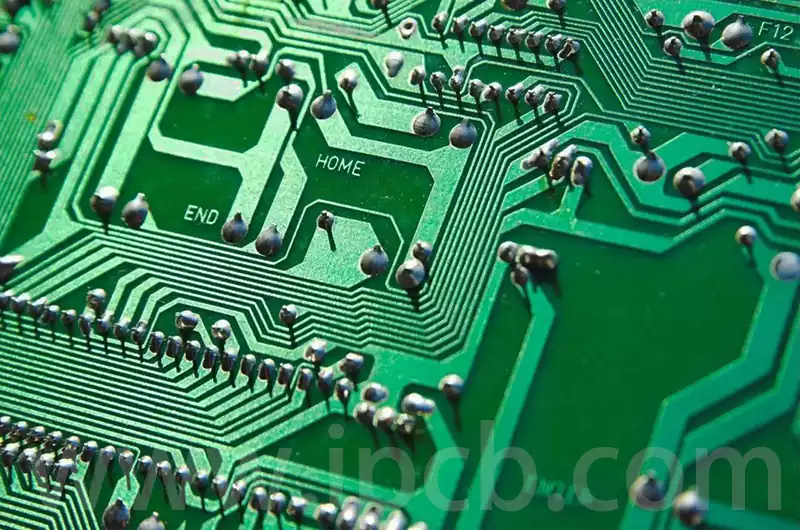
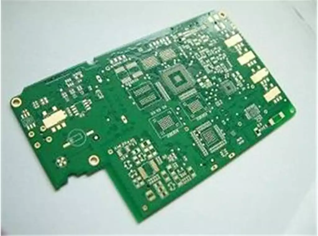
High speed PCB is mainly used in high-speed digital circuits where signal transmission integrity needs to be ensured. High-frequency PCBs are mainly used in high-frequency (frequency above 1GHz) and ultra-high-frequency (frequency above 10GHz) electronic devices, such as RF chips, microwave receivers, RF switches, air-space tuners, frequency selective networks and so on. Unlike high-frequency PCBs, the design of high-speed PCBs requires more consideration of factors such as signal integrity, impedance matching, signal coupling and signal noise. In order to meet these requirements, high-speed PCBs need to use special materials and adopt special processes. In high-speed PCB design, it is crucial to choose the right high-speed CCL material.
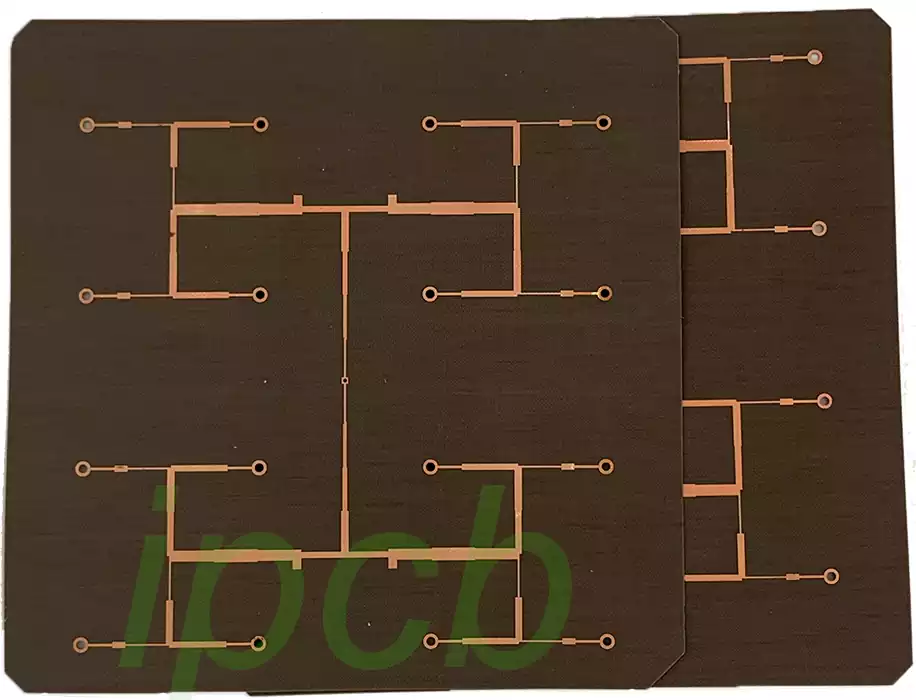
Copper clad laminate (CCL) as the core substrate material in PCB manufacturing, the PCB mainly plays the role of interconnecting conduction, insulation and support, and has a great influence on the signal transmission speed, energy loss and characteristic impedance in the circuit, etc. The technological development trend of the CCL is consistent with the technological development trend of the PCB, which is mainly embodied in the aspects of miniaturization, high-level, flexibilization and intellectualization, etc. For example, HDI boards and class carrier boards have a high speed. For example, HDI boards and class carrier boards require higher micro-miniaturization capability of CCL; high multilayer through-hole boards and backplanes require higher number of layers and structure of CCL; flexible boards and rigid-flex combination boards require higher flexibility and reliability of CCL; package substrates and embedded component boards require higher integration and intelligence of CCL.
High speed PCB design process
Overall circuit analysis of the single board: the single board of the main chip program, power supply program, the main bus, signal flow, power tree, interface types, process programs, EMC programs, etc. to do the overall understanding and planning
Pre-layout, pre-simulation analysis: In comprehensive consideration to meet the signal quality, EMC, thermal design, DFM and other aspects of the basis of the main devices reasonably placed on the PCB substrate. Layout and wiring: In order to meet the requirements of signal quality, DFM, EMC and other rules, complete the device placement and signal interconnection.
Post-simulation verification: SI simulation, PI simulation, thermal simulation.
Process review: DFM using advanced tools such as Valor.
Impedance control in high speed PCB design
The three factors that affect impedance control are the substrate material, the width of the alignment and the height of the alignment from the ground/power layer.
At low frequencies the PCB board track is defined by DC characteristics and is considered an ideal circuit with no resistance, capacitance or inductance. As frequency increases, the inductance and capacitance associated with the track begins to affect performance. Alignment impedance mismatches due to over-hole stubs and alignment defects can result in signals not being fully absorbed within the receiver.
At these high data rates, this can lead to signal overshoot, undershoot, and ringing, resulting in signal errors. To solve this problem, the transmission line provides a ground plane and termination resistor underneath. Impedance mismatch can be controlled by implementing an appropriate termination scheme, depending on the specific application.
- Parallel Termination Scheme
In this scheme, the termination resistance (RT) is equal to the line impedance. The terminating resistor is placed as close to the load as possible to maximize efficiency, and the current loading of the terminating resistor is maximized at high output. - Davenant Termination Scheme
The Davenant termination scheme is an alternative to the parallel termination scheme where the termination resistor (RT) is split into 2 separate resistors equal to the line impedance. This scheme reduces the total current drawn from the power supply and increases the current drawn from the power supply because the resistor is placed between the UCC and ground. - Active parallel termination
In active parallel termination, the termination equivalent to the line impedance (Z0) is placed in the path of the bias voltage, which is arranged so that the output driver can draw current from high levels and levels. This scheme requires a separate voltage source that can be potted into and pulled out of the circuit to match out transmission rate. - Series-RC Parallel Termination
In series-RC parallel termination, a combination of resistor and capacitor (>100pF) acts as the termination impedance, where the termination resistance (RT) is equal to Z0, and the capacitor blocks the low-frequency signals and passes the high-frequency components, so that the DC loading effect of RT does not affect the driver. - Series Termination
Match the impedance of the signal source, not the load. This scheme helps to attenuate secondary reflections, and the line impedance varies according to the distribution of the load. A single resistor value does not apply to all conditions, and the method requires only one component at the source rather than multiple components at each load, but delays the signal path by increasing the RC time constant. - Differential Pair Termination
A termination resistor is required between the signals at the receiving end. The termination resistor must match the differential load impedance (typically 100Ω)
With the rapid development of modern electronic technology, the importance of high-speed PCB design in the field of electronic engineering has become increasingly prominent. In high-speed digital circuits, it is not only to ensure the integrity of signal transmission, but also need to deal with signal integrity, impedance matching, signal coupling and signal noise and many other challenges. In order to meet these challenges, designers need to study the material properties in depth, optimize the layout and wiring, and accurately control the impedance in the design.
Copper clad laminate (CCL) as the core substrate material in PCB manufacturing, its technological development trend is closely linked to the technological development of PCB. Choosing the right CCL material is critical to enhancing its performance. Meanwhile, in the high-speed PCB design process, from the overall circuit analysis of the single board to pre-layout, pre-simulation analysis, to layout and wiring, post-simulation verification and process review, each step needs to be operated in a delicate way to ensure the successful implementation of the design.
High speed PCB design is a task full of challenges and opportunities. Through in-depth study of material properties, optimization of the design process, and precise control of impedance, we can continuously improve its performance and provide strong support for the development of modern electronic technology.