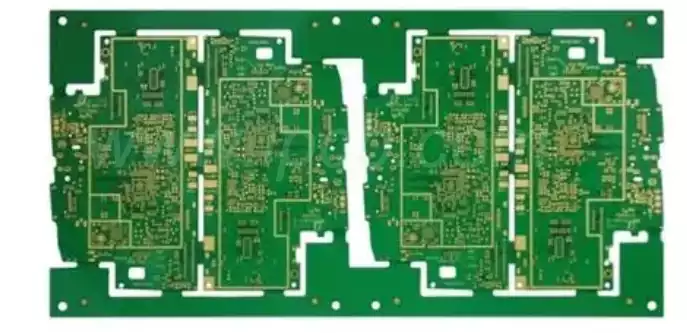
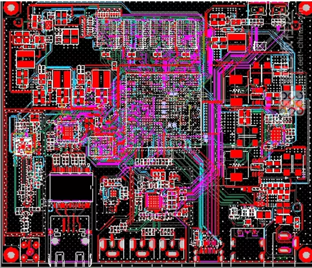
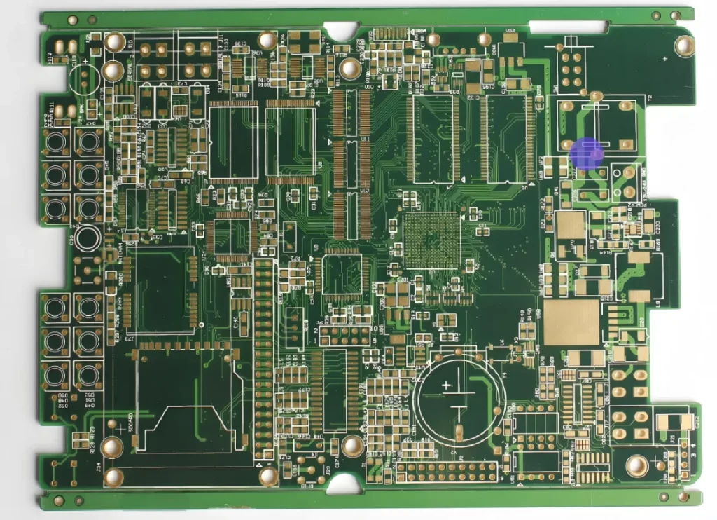
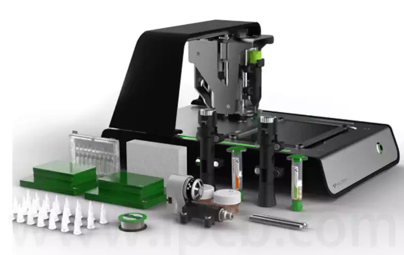
ELIC PCB is one of the HDI products, the full name is every layer interconnection, is the highest end of the HDI products. ELIC boards are commonly stacked for 8 to 14 layers.
Any layer interconnection (ALIVH) technology, as the name suggests, is a multi-layer printed circuit board (PCB) can be achieved in any two layers of the connection between the advanced manufacturing technology. This technology not only breaks through the limitations of traditional HDI (High Density Interconnect) technology in the interlayer connection, but also greatly improves the integration and performance of the circuit board. ALIVH technology allows designers to freely lay out circuits in a limited physical space according to the actual needs, thus achieving more complex and efficient circuit design.
The realisation of ALIVH technology is a complex and delicate process that relies on the close collaboration of several key process technologies. Such as interlayer alignment technology, fixed shrinkage preset, conductive filling, laser drilling technology and so on.
ELIC PCB has the following advantages over traditional PCBs:
High Density Integration: Using a multi-layer structure, ELIC PCBs are able to integrate more circuit components in a smaller space, achieving a high density layout. This is critical for modern electronic devices, especially portable devices such as mobile phones and tablets.
Good electrical performance: ELIC PCB is made of special materials with low resistance and consumption, which maintains excellent signal integrity and reduces signal attenuation under high-frequency operating conditions.
Reduced Signal Interference: Through electrical design optimisation, ELIC PCBs are able to effectively reduce signal crosstalk and interference, improving circuit stability and reliability.
Flexible Design Capability: ELIC PCB’s manufacturing technology allows for more complex and flexible designs that can be easily adapted to different product requirements while supporting the integration of smart features.
ELIC (Every Layer Interconnect) PCB manufacturing process
An ELIC PCB is a printed circuit board that offers a number of advantages over traditional PCBs. It is constructed from multiple layers of interconnect material, providing greater flexibility in circuit routing. This design not only reduces the overall footprint of the board, but also reduces signal integrity issues such as crosstalk.
ELIC PCBs are typically fabricated using a sequential lamination process, in which multiple layers of material are tightly bonded by applying heat and pressure. The following is a brief overview of the sequential lamination process and the challenges associated with manufacturing ELIC PCBs.
Building the Stack
The first step in the sequential lamination process is to build the individual layers that make up the ELIC PCB, which typically has between two and eight layers, although four- or six-layer boards are more common. Each stack consists of a different material, insulator or conductor. Once the stack has been constructed, it is placed in a laminator for the next step.
Lamination Processing
The laminator applies the right amount of heat and pressure to the layers to make them fit together. The amount of heat and pressure required depends on the type of material used. For example, insulating materials typically require less heat and pressure than conductive materials. The lamination process can typically be completed in approximately one hour.
Line Etching
After the ELIC PCB is laminated, a line etch is performed. Line etching is the process of removing unwanted material from the board to create the desired circuit pattern. This process is usually carried out using a chemical solution and a stencil is used to apply the solution to the board. The stencil has the design of the circuit printed on it and the chemical solution etches away the exposed areas of the board.
Finished Product Processing
The final step in the ELIC PCB manufacturing process is to apply a surface treatment. The most common surface finishes are soldermask and overlay. Soldermask is a thin layer of polymer applied to the top and bottom of the board, while overlay is a thin layer of adhesive applied to the top of the board. Both treatments protect the circuitry from damage and contamination.
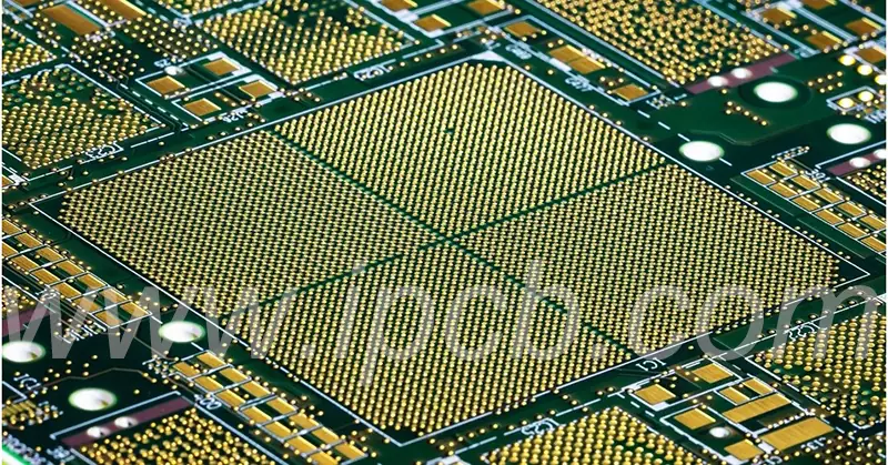
Cost Comparison between ELIC PCBs and Conventional PCBs
- Material Costs
ELIC PCB: Special materials with high frequency and high dielectric constant, such as polyimide and high performance FR4 materials, are usually used. These materials are more expensive compared to traditional PCB materials (e.g. ordinary FR4), so the material cost of ELIC PCB is usually higher.
Traditional PCB: Widely used ordinary FR4 material, which is relatively low cost and suitable for low-cost applications in mass production.
- Design and manufacturing process complexity
ELIC PCB: Using multi-layer structure and fine microvia technology, the design and manufacturing process is more complex. This complexity requires a higher level of technology and equipment investment, and the associated design and development costs increase significantly.
Conventional PCB: Usually single or double layer structure, relatively simple manufacturing process, short development cycle, lower design cost.
- Production efficiency
ELIC PCB: Certain steps in its manufacturing process, such as laser drilling and chemical copper plating, enhance the board’s performance but may also extend the production cycle, resulting in higher costs per unit of output.
Conventional PCB: Due to the maturity of the process and the efficiency of the production process, it is able to respond quickly to market demand, which usually reduces the overall production cost.
- Economies of scale
ELIC PCB: Due to its high performance positioning, it usually targets specific high-end applications. Production quantities are relatively small, making it difficult to form economies of scale, resulting in higher average costs.
Traditional PCB: Due to its wide range of applications, especially in consumer electronics, the production volume is large, which can effectively achieve economies of scale and reduce unit costs.
ELIC PCB, as the highest-end product in HDI technology, plays a pivotal role in modern electronic equipment by virtue of its high-density integration, good electrical performance, reduced signal interference and flexible design capabilities. Especially in mobile phones, tablet PCs and other portable devices, the advantages of ELIC PCBs are more prominent, providing more complex and efficient circuit design solutions for these devices.
However, while ELIC PCB bring many advantages, they also come with higher costs. From the cost of materials, design and manufacturing process complexity, production efficiency to economies of scale, ELIC PCB costs are higher than traditional PCBs, which makes ELIC PCBs are mainly positioned in high-end applications, while traditional PCBs are more suitable for mass production of low-cost applications.
