Preparing a printed circuit board (PCB) is a critical step in the electronics design and manufacturing process. Whether you’re creating a simple circuit for a hobby project or a complex board for an industrial application, understanding the preparation steps is essential for ensuring the final product meets your specifications and performs reliably. This article will guide you through the comprehensive process of how to prepare PCB board, focusing on key stages from design to fabrication and assembly.
Understanding PCB Basics
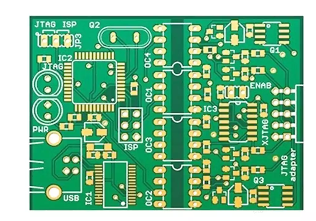
Before delving into the preparation process, it’s essential to understand what a PCB is. A printed circuit board is a board used to connect electronic components through conductive pathways, etched from copper sheets laminated onto a non-conductive substrate. The PCB serves as a foundation for electronic circuits, allowing for the integration of various components, such as resistors, capacitors, and integrated circuits.
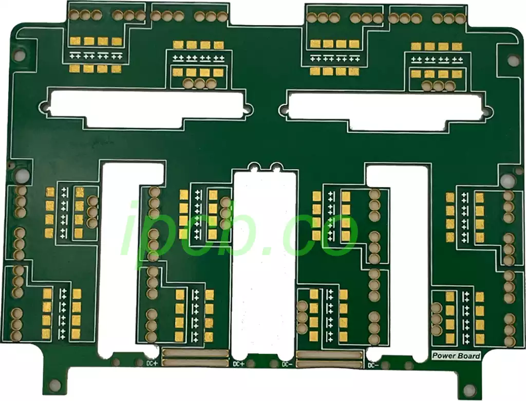
PCBs come in various types, including single-sided, double-sided, and multi-layer boards. The type of PCB you choose will depend on the complexity of your project, the number of components you need to accommodate, and the required electrical performance. For instance, single-sided PCBs are simpler and more cost-effective, while multi-layer PCBs allow for more complex designs and higher component density.
Types of PCBs
- Single-Sided PCBs: These boards have components mounted on one side and conductive pathways on the other. They are used for simple applications like calculators and LED lights.
- Double-Sided PCBs: These boards have conductive pathways on both sides, allowing for more complex circuits. They are commonly used in devices like radios and televisions.
- Multi-Layer PCBs: These boards consist of multiple layers of conductive material, allowing for complex designs with high component density. They are used in advanced electronics like smartphones and computers.
Step 1: Designing the PCB Layout
The first step in how to prepare PCB board is designing the layout. This phase involves creating a schematic that represents the electronic circuit and translating it into a physical layout on the PCB. Here are the key considerations for PCB design:
Schematic Design
Begin by creating a schematic diagram using PCB design software such as Eagle, Altium Designer, or KiCad. The schematic should include all the components, their connections, and any relevant specifications. Pay attention to the following:
- Component Selection: Choose components that suit your design requirements. Ensure they are readily available and fit within your budget. Consider factors such as power ratings, sizes, and compatibility with your PCB layout.
- Net Connections: Clearly define the electrical connections (nets) between components to avoid errors in the layout. A well-structured schematic can significantly reduce mistakes during the layout phase.
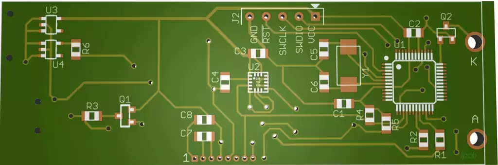
PCB Layout Design
Once the schematic is complete, you can start laying out the PCB. This involves placing components on the board and routing the connections. Key factors to consider include:
- Component Placement: Position components logically to minimize trace lengths and avoid interference. Group related components together to enhance performance. For example, keep power components close to the power supply and signal components together.
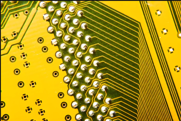
- Trace Width and Spacing: Determine appropriate trace widths based on current-carrying capacity and spacing to prevent short circuits and signal integrity issues. Use appropriate design rules to ensure traces are wide enough for the required current.
- Layering: If using a multi-layer PCB, plan the stack-up configuration. This affects impedance control, signal integrity, and power distribution. Consider using dedicated ground and power planes to enhance performance.
Step 2: Preparing the Gerber Files
After completing the PCB layout, the next step in how to prepare PCB board is generating Gerber files. These files contain the necessary information for PCB fabrication, including layer details, drill files, and solder mask definitions.
Generating Gerber Files
Use your PCB design software to export Gerber files. Ensure to include the following:
- Copper Layers: Files for each copper layer, including traces and pads. Ensure all layers are correctly formatted for the manufacturer.
- Solder Mask Layers: Files indicating where the solder mask will be applied, protecting non-solder areas. Proper solder mask application is crucial for preventing solder bridges.
- Silkscreen Layers: Files containing text and graphics for component designations and logos. This helps with assembly and troubleshooting.
- Drill Files: Information on hole sizes and locations for through-hole components. Ensure drill files are compatible with the manufacturer’s specifications.
Verification
Before sending the Gerber files to a manufacturer, verify their accuracy. Many PCB design tools offer a built-in design rule check (DRC) to identify potential issues. Additionally, use a Gerber viewer to visually inspect the files for errors. This step is vital to catch mistakes before production, as changes can be costly.
Step 3: Selecting a PCB Manufacturer
Choosing the right PCB manufacturer is crucial to the success of your project. Different manufacturers offer varying levels of service, quality, and pricing. Here are key considerations when selecting a manufacturer:
Manufacturing Capabilities
Ensure the manufacturer can produce the type of PCB you need, whether it’s single-sided, double-sided, or multi-layer. Check their capabilities regarding:
- Material Options: Confirm they use suitable materials for your application, such as FR-4, Rogers, or aluminum. The choice of material affects performance, durability, and cost.
- Layer Count: Verify they can handle the required number of layers for your design. Not all manufacturers support high-layer counts, which can limit your options.
- Special Requirements: Inquire about capabilities for blind/buried vias, controlled impedance, or other specific features. If your design requires specialized manufacturing techniques, ensure the manufacturer can accommodate them.
Quality Assurance
Look for manufacturers with a strong reputation for quality. Certifications such as ISO 9001 or IPC-A-600 demonstrate adherence to industry standards. Request samples or references to evaluate their work. This step can save you time and money by ensuring high-quality production.
Cost and Lead Time
Compare quotes from different manufacturers to find a balance between cost and quality. Be sure to consider the lead time, especially if you have a tight project deadline. Understand the trade-offs between price and speed, and factor in any additional costs for expedited services.
Step 4: Fabrication Process
Once you’ve selected a manufacturer, the next phase in how to prepare PCB board is the fabrication process. Here’s what to expect:
PCB Fabrication Steps
- Material Preparation: The manufacturer starts with a base material, typically a copper-clad laminate. This material is cut to the desired size. The choice of laminate affects the board’s electrical properties and mechanical strength.
- Etching: The manufacturer applies a photoresist layer to the copper and uses UV light to expose the design. The exposed areas are etched away, leaving behind the copper traces. This process requires precision to ensure clean, accurate traces.
- Drilling: Holes are drilled for through-hole components and vias, as defined in the Gerber files. The accuracy of this step is critical for proper component placement and connectivity.
- Plating: For multi-layer boards, the manufacturer plates the inner layers to create conductive paths between them. This process is essential for ensuring reliable electrical connections.
- Solder Mask Application: A solder mask is applied to protect the copper traces from oxidation and to prevent solder bridges during assembly. The solder mask is crucial for the longevity of the PCB.
- Silkscreen Printing: Component designators, logos, and other markings are printed on the board. This aids in assembly and troubleshooting, making it easier to identify components.
- Final Inspection: The manufacturer conducts a thorough inspection of the finished PCBs to ensure they meet quality standards. This step may include electrical testing and visual inspections.
Step 5: Assembly Preparation
After fabrication, the next step in how to prepare PCB board is assembly. This involves placing components on the PCB and soldering them in place.
Component Sourcing
Before assembly, procure all necessary components. Ensure they match the specifications outlined in your design. Consider the following:
- Lead Time: Be aware of the lead time for components, especially for custom or specialized parts. Timely sourcing can prevent delays in your project.
- Supplier Reliability: Source components from reputable suppliers to avoid counterfeit parts. Verify the authenticity of components to ensure performance and reliability.
Assembly Techniques
Depending on your project, you can choose between manual and automated assembly:
- Manual Assembly: Suitable for small batches or prototypes. It involves hand-soldering components onto the PCB. Manual assembly allows for greater flexibility and control, especially in early development stages.
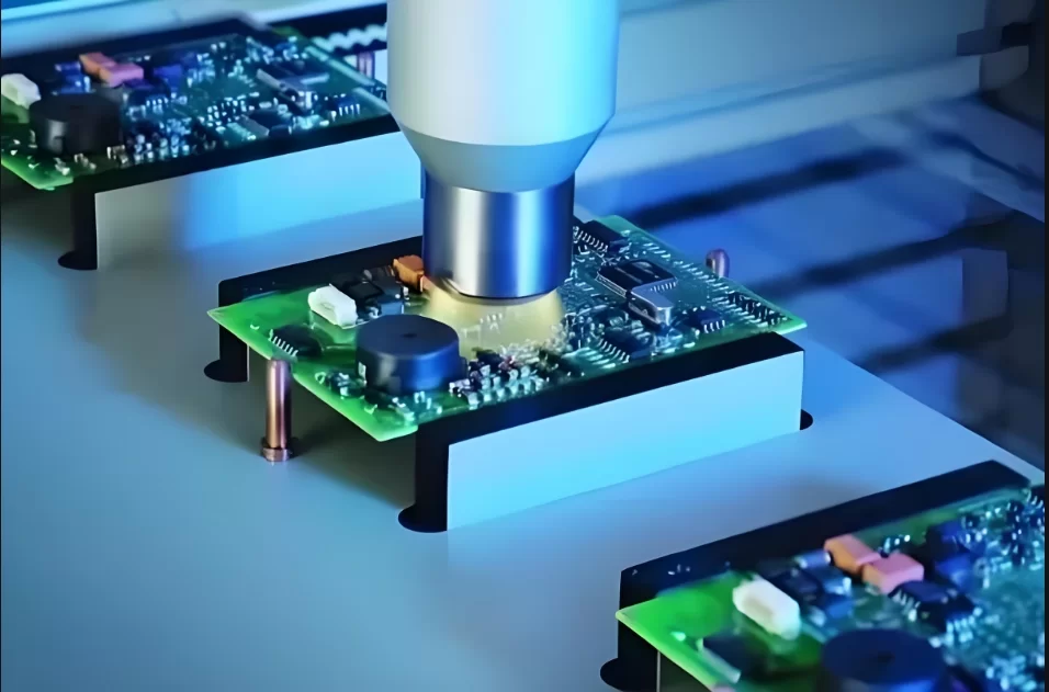
- Automated Assembly: For larger production runs, automated pick-and-place machines can efficiently position and solder components. Automated assembly increases consistency and speed, making it ideal for mass production.
Testing and Quality Control
After assembly, it’s crucial to test the assembled PCB to ensure it functions as intended. Implement a testing protocol that includes:
- Functional Testing: Verify that the circuit operates correctly under expected conditions. Testing should encompass all functional aspects of the circuit.
- In-Circuit Testing (ICT): Check for manufacturing defects and ensure component values are within specifications. ICT can detect problems such as incorrect component placement or faulty solder joints.
- Environmental Testing: Consider conducting tests under various environmental conditions to ensure the PCB performs reliably under real-world conditions. This may include thermal cycling, humidity exposure, and vibration tests.
Step 6: Final Inspection and Testing
Once the assembly is complete, it’s essential to conduct final inspections and tests to ensure the PCB functions correctly and meets all specifications.
Final Inspection
Perform a detailed visual inspection of the assembled PCB. Check for:
- Solder Joints: Ensure solder joints are clean and free of defects, such as cold solder joints or solder bridges. Proper soldering techniques are critical for reliable connections.
- Component Orientation: Verify that all components are correctly oriented and securely mounted. Misplaced components can lead to circuit failures.
- Physical Damage: Inspect the board for any signs of damage that may have occurred during handling or assembly.
Comprehensive Testing
Conduct thorough testing to ensure the PCB operates as expected. This may include:
- Functional Testing: Check the circuit’s performance under normal operating conditions to verify all features function as intended.
- Electrical Testing: Measure voltage, current, and resistance to confirm the circuit meets specifications. Identify any discrepancies that may indicate issues.
- Stress Testing: Evaluate the board’s performance under extreme conditions, such as high temperatures or voltages, to ensure reliability.
Conclusion
In summary, preparing a PCB board involves multiple critical steps, from initial design to final inspection. Understanding how to prepare PCB board is essential for anyone involved in electronics design and manufacturing. By following the outlined steps, you can ensure that your PCB meets all specifications and performs reliably in its intended application.
Whether you’re a hobbyist working on a small project or an engineer involved in large-scale production, mastering the preparation process will greatly enhance the quality and success of your electronic designs. With careful attention to detail at each stage, you can create PCBs that meet the demands of today’s advanced electronic applications.
In the end, proper preparation can significantly impact the performance, reliability, and overall success of your electronic devices. Emphasizing quality in each step, from design to testing, will yield better results and enhance your reputation in the competitive PCB industry.