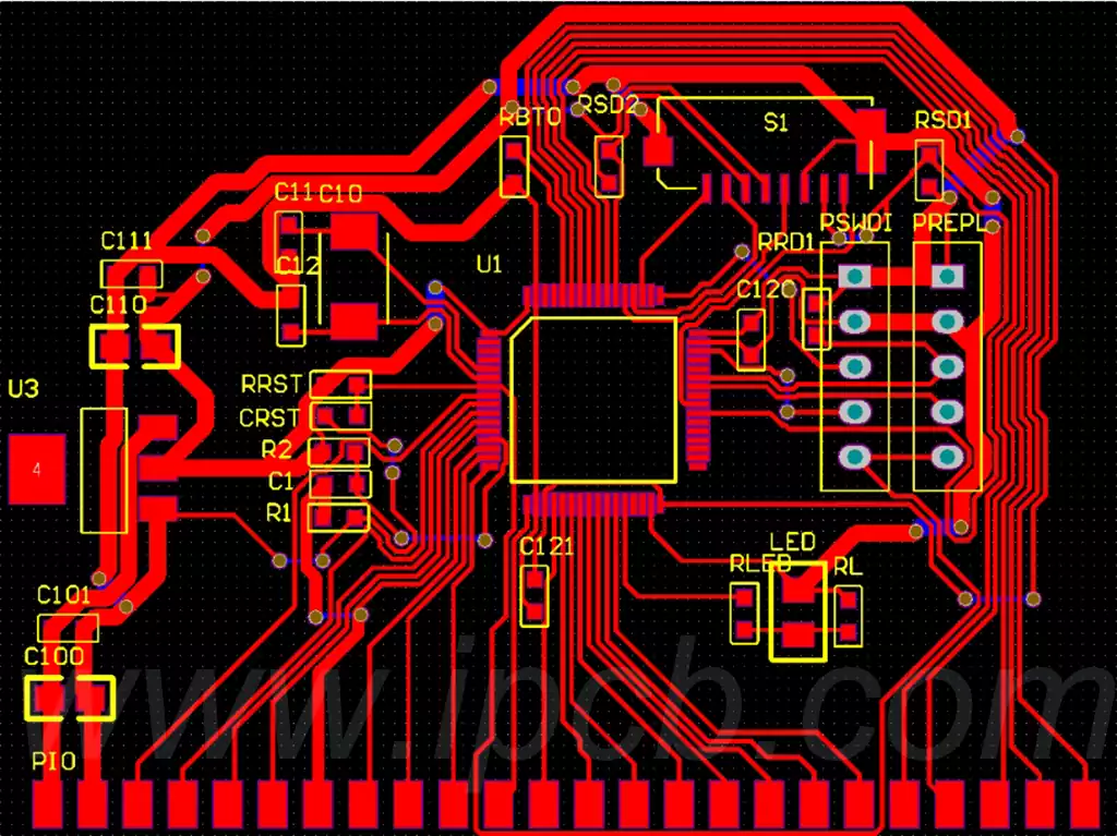
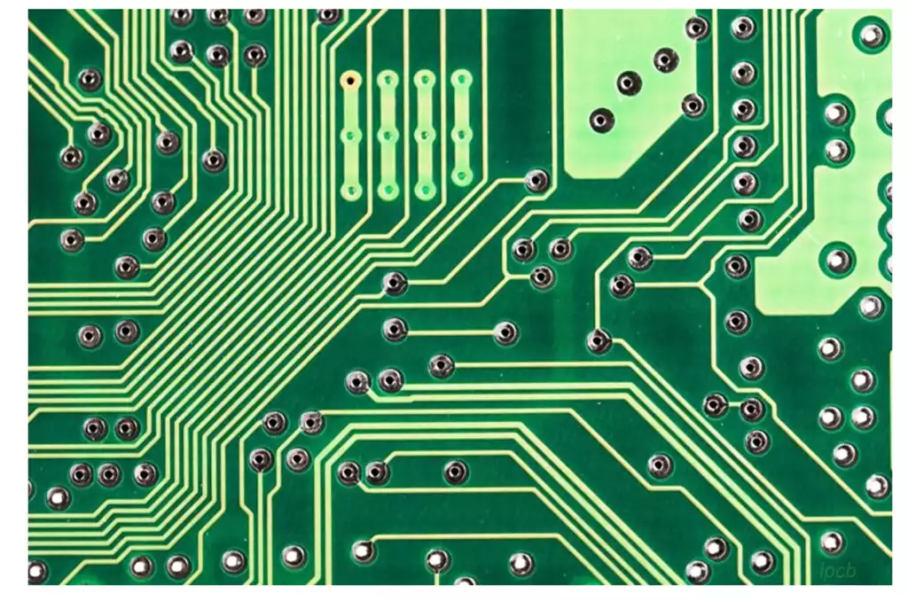
PCB diagrams, which are mapped drawings of circuit boards, depict in detail the circuit board’s alignment, the location of components, and so on. How to read a circuit board has become a threshold that every electronic engineer must cross.
How to read a circuit board:
Familiarise yourself with the general working principle, workflow and signal flow of the circuit board, as well as the location of each major and core component on the printed circuit board (PCB).
It is recommended to view the PCB in terms of signal flow. It is possible to trace forward (e.g. starting from the tuner and looking backwards) or backward (e.g. starting from the speaker and looking backwards), and sometimes a combination of both is required to analyse certain circuits. Circuits will often have branches, and it is necessary to look at each branch separately. If there are too many branches, you can mark them to distinguish between viewed and unviewed branches, and pause at the marked position to view the rest of the circuit first. When the analysis returns to the original pause point, then continue to analyse that part of the circuit.
It is a good idea to determine the orientation of the power and earth wires first and note the location of these as you view them. When analysing components, it is important to be aware if one end of the component is connected to a power or earth wire, even if that part of the circuit has been analysed. The edges of the board, the strip of copper foil with the largest area, where the heat sink connects to the copper foil, etc. (usually the negative side) are all grounds. If these features are not obvious, look at the power supply’s filter capacitor (for positive power supplies), i.e., the negative connection of the electrolytic capacitor is the circuit’s negative or ground.
Along the signal flow, when encountering unit circuits or functional circuits, the core components such as transistors and integrated circuits (ICs) should be viewed as the centre of the circuit, looking in turn at the components and connecting wires connected to each pole of the transistor, as well as the components and circuits around the pins of each IC. Of course, it is also possible to divide the entire board into several parts and then analyse them one by one. While looking at the parts, analyse what they do and how the signals change (it’s a good idea to consider possible malfunctions that may occur if a part is damaged). When encountering unfamiliar circuits, you need to figure out their composition and circuit characteristics, and then contact similar typical circuits for comparison, viewing and analysis.

Have a soldering iron and multimeter ready when looking at a circuit board, as when encountering a transistor you need to know whether it is NPN or PNP type and the pin order of each pole helps to analyse the circuit. With a lot of experience, it is possible to determine the type of transistor and the position of each electrode when viewing most circuit boards. Sometimes it is necessary to identify circuit connections based on the internal structure of components (e.g., switches, potentiometers, centre circles, etc.), and these need to be measured.For double-sided (multilayer) assemblies, some traces and vias are often covered, which require measurements or even removal of the assembly for visual observation.
Beginners must draw a schematic at the same time they view the PCB. When drawing the schematic, each component should be labelled with its number to avoid omissions or misunderstandings and to correct errors in a timely manner. If the component is on the front side (for a single panel, but there are surface mount components on the back side as well),its trace pads are on the reverse side. Remember that when the front side is facing up, the reverse side is facing the opposite direction. For example, the capacitor on IC pin 1 (assuming it’s on the left side of the IC) should be seen in the opposite position on the reverse side when it’s on the right side of the IC component.
There are also some lessons to be learnt: for example, a rectifier diode about 10 mm long is placed horizontally on the front side,and it is also placed horizontally on the reverse side, but with the orientation of the positive and negative terminals changed. To find the pads and pinholes of this component on the reverse side, one can first observe its approximate position. On the reverse side, you can see two holes in the horizontal position, which are 10 mm apart and slightly larger than the diode feet, which are the holes for this component. (When there is no other diode next to this diode.) In other words, when looking for the location of the pinhole for the negative component, you can judge it based on some of the characteristics of the component itself and its relative position to other components. If the PCB components are arranged horizontally and vertically, and you see a hole on the reverse side that is tilted and has another hole next to it, do not mistake it for the two legs of a particular component.
For ease of analysis, some printed circuit boards have blue or green strips printed on the front side in the same shape as the copper foil strips on the back side, or the symbols and numbers of the components are printed on the reverse side (single-sided copper foil soldered side). With such boards, the former can be analysed for most circuits by looking at the front side only, while the latter can be analysed for almost the entire board by looking at the back side only. This avoids the hassle of flipping back and forth and errors caused by confusion.
In short, to understand the exact process of circuit boards, you can choose some simple and familiar boards to view and draw before viewing complex PCB boards.How to read a circuit board is an indispensable skill for electronic engineers, it requires both theory and practice, patience and meticulous coexistence.


