IC chip fabrication is a complex and delicate process involving multiple steps, from design to production and ultimately packaging.Its essence is the integration of various electronic components onto a single piece of semiconductor material (usually a silicon wafer) to realize a specific circuit function.
Core Processes of IC Chip fabrication:
1.IC chip design
The first step in IC chip fabrication is the design phase.In this phase,engineers use a hardware description language (e.g., VHDL or Verilog) to describe the function of the chip, and perform logic design and circuit design.After the design is complete, layout and routing (Layout) are performed with design tools to ensure the physical realization of the circuit.
Logic design: Determine the functions that the chip should realize.
Circuit design: Design the circuit diagram and select appropriate logic gates and modules.
Layout and wiring: Generate the physical layout according to the circuit design and plan the areas and connections inside the chip.
2.Photomask Production
When the design is complete, the next step is to create a mask.A mask is a template used in the lithography process that contains the pattern of the chip design. The process of making a mask involves high-precision lithography and is usually based on a silicon wafer (Wafer).
Photolithography process: A light source is used to transfer the design pattern onto the silicon wafer,utilizing a photosensitive adhesive to form the desired pattern.
Photomask Calibration: Ensuring that the pattern in the photomask matches the actual design is a critical step in the manufacturing process.
3.Wafer Processing
After obtaining the photomask, the silicon wafer processing stage begins. This stage usually consists of several steps, including doping, oxidation, etching and deposition processes.
Doping: Impurities are introduced into the wafer through ion implantation to change its conductivity.
Oxidization: Creates a silicon oxide layer on the surface of the wafer to protect the chip and form an insulating layer.
Etching: Removal of unwanted material to realize the desired circuit structure.
Deposition: Deposits metallic material on a silicon wafer to form connecting circuits.
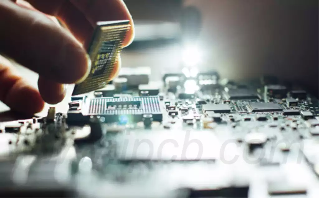
4.Packaging
After the chip has been processed, it needs to be packaged. Packaging not only protects the chip from the external environment, but also ensures the connection between the chip and other electronic components.
Package type: Common package types include DIP, SOP, BGA and so on. Choosing the right type of package depends on application requirements and cost considerations.
Soldering and Testing: During the packaging process, the chip will be soldered to the substrate and initial testing will be performed to ensure proper functionality.
5.Mass Production and Testing
After completion of the package, the chip will enter the mass production stage.At this point,rigorous testing must be carried out to ensure that the performance and quality of each chip meets the standards.
Functional test: Verify the accuracy and reliability of the chip function.
Performance testing: Test the performance of the chip under different operating conditions,such as temperature, speed and current.
Failure analysis: Analyze the chip that fails the test to find out the cause of failure in order to improve the design and manufacturing process.
The most commonly used test methods in the test phase of IC chips:
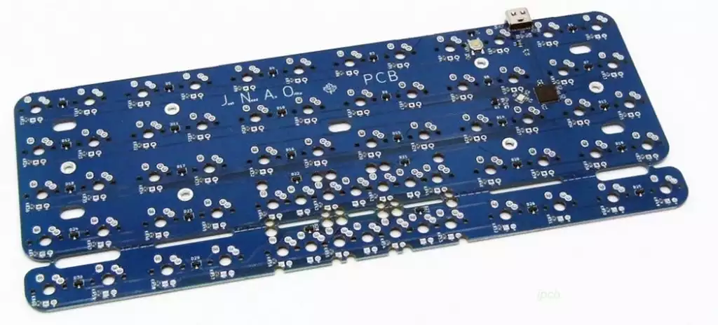
1.Board level test
Board level testing is an important part of IC chip testing,mainly applied to functional testing.The test usually uses a PCB board and a chip to build a test module to ensure that the chip operates according to the design specifications through electrical parameter testing and functional verification.
- Wafer Test (CP Test)
Wafer test, also known as CP (Chip Probing) test is mainly in the chip has not been packaged,the use of test equipment to evaluate its electrical performance. This method can screen out defective chips in advance, reducing the cost and risk of subsequent packaging. - Finished product test (FT test) after packaging
Finished product test (FT) is a comprehensive test of the chip after packaging is completed.The test is designed to confirm the performance of the chip in the actual working environment, including functional testing and stability testing to ensure that it meets factory standards. - System Level Test (SLT Test)
System level test is conducted after the whole system is assembled to test the performance of the chip in actual applications and interface functions. This test can help identify potential problems caused by the whole system environment. - Reliability Test
The main goal of reliability testing is to evaluate the performance of IC chips under different operating conditions, including high temperature, high humidity, vibration and other extreme environmental factors. Such testing usually involves accelerated aging tests to predict the life cycle and durability of the chip. - Other Testing Methods
In addition to the main testing methods mentioned above, there are some commonly used additional testing methods, such as static testing, dynamic testing, temperature testing and insulation testing. These methods can help to further confirm the chip’s electrical characteristics, functionality and operational stability under various environmental conditions.
The IC chip fabrication and testing process embodies a complex and delicate process.From circuit logic at the design stage,through photomask fabrication and silicon processing, to packaging and mass production, each step is critical to ensure product performance and reliability.Through rigorous testing methods, including board-level testing, wafer testing and post-packaging testing, engineers are able to identify and resolve potential problems in a timely manner, ensuring the stability and long-term reliability of the chip in real-world applications. As technology advances and needs diversify,IC chip fabrication and testing processes will continue to evolve to meet the growing standards and challenges of the electronics industry.