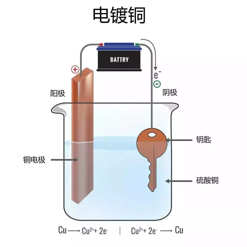
PCB assembly is the process of combining a circuit board with other electronic components (e.g., connectors, housings, heat sinks, etc.) to be embedded in the final product.
PCB Assembly Design Tips
1.Pay attention to the gap between components One of the most common issues raised by PCB Layout gurus: component-to-component spacing. Two components that are too close to each other can create a variety of problems that may require redesign and remanufacturing, resulting in a loss of time and money.
As a general rule, wiring and layout rules generally require, for example, that the minimum spacing between discrete components such as capacitors and resistors be at least 10 mils, with 30 mils being the preferred spacing.
2.In the design phase on the choice of components experienced PCB Layout engineers in the early stages of the design will be a good choice of components, which can ensure that the design and the actual assembly will not appear too much conflict. At the outset, consider the size of the components, space, in the PCB assembly process will not have so many problems. Generally speaking, smaller components take up less space on the PCB, so we need to consider whether it is possible to reduce the size of the components.
3.Separate leaded components from lead-free components Be sure not to mix lead-free components with components that are leaded. If any component requires lead-free assembly and there are no available alternatives to traditional leaded solder, the entire PCB must be assembled lead-free and all components must comply with lead-free assembly requirements. Sometimes the only package available for a particular device is a Pb-free BGA, but usually there are some specific requirements. Separation tabs left between PCBs after wiring interferes with assembly of connectors that extend to that edge. the following problems occur when board manufacturing and assembly are not closely coordinated.
4.Place large assemblies evenly Distribute large components as evenly as possible on the PCB board during layout for optimal heat distribution during reflow. Make sure the PCB manufacturer develops a reflow profile for the amount of reflow.
5.Do not place SMD components too close to the edge of the PCB. It is best to place SMD components 150 mils (3.8 mm) away from the edge, especially if V-grooves are used.
6.Do not use very small drills like 6 mil drilling is almost the smallest mechanical drill and is not recommended unless there is no other choice. Due to BGA densities, 18.5/8 (18.5 mil pads/8 mil drill holes) is recommended, ideally 22/10 would be good, but BGA does not allow it. (Figures are for reference only and are subject to change)
How to assemble a pcb board
Simply put, the PCBA process is actually SMT processing process + DIP processing process.
Process, PCBA process processing flow can be roughly divided into five main links, respectively:
SMT chip processing → DIP plug-in processing → PCBA test → three anti-coating → finished product assembly
SMT chip processing process is: solder paste mixing → solder paste printing → SPI → mounting → reflow soldering → AOI → rework
SMT chip processing link will generally be based on the customer’s BOM list provided by the components to match the purchase, confirm the production of PMC program. After the preparatory work is completed, the SMT programming will begin, according to the SMT process, the production of laser stencils, solder paste printing.
Through the SMT mounter,components are mounted onto the circuit board, and if necessary, in-line AOI automatic optical inspection is performed.After inspection, a perfect reflow oven temperature profile is set and the board is allowed to flow through reflow.
After the necessary IPQC inspection,the DIP insertion process can then be used to pass the inserted material through the board and then flow through the wave soldering for soldering. Then comes the necessary post-oven process.
In the above processes are completed, but also QA comprehensive testing to ensure product quality.
1.Solder paste mixing will be taken out of the refrigerator after thawing, the use of hand or machine for mixing, in order to be suitable for printing and soldering.
2.Solder Paste PrintingPlace the solder paste on the stencil and print the solder paste or SMD adhesive onto the PCB pads by squeegee to prepare the components for mounting.
3.SPISPI that is, solder paste thickness detector,can detect the situation of solder paste printing,and play a role in controlling the effect of solder paste printing.
4.Placement of SMD components placed on the Flyer,the head of the SMD machine through the identification of the components on the Flyer accurately mounted on the PCB pads in a fixed position. (Generally used Yamaha mounter, Panasonic mounter)
5.Reflow soldering
Will be mounted on the PCB board over the reflow soldering,after the role of high temperature inside the solder paste melting, so that the paste paste heat into liquid, and finally cooled and solidified to complete the welding.Make the surface mount components and PCB firmly brazed together to achieve the electrical performance required by the design and in full accordance with international standards curve precision control, can effectively prevent thermal damage and deformation of PCB and components. The equipment used for reflow oven (automatic infrared / hot air reflow oven), located in the SMT production line in the back of the placement machine.
6.AOI inspection (automatic optical AOI detector) AOI that is, automatic optical inspection, its role is to scan the PCB board mounted on the welding quality and assembly quality inspection. The equipment used has a magnifying glass, microscope, location according to the needs of the inspection, can be configured in the production line in the right place.
7.Rework
AOI or manually detected defective rework. Its main role is to detect faults in the PCBA rework, such as tin ball, tin bridge, open circuit and other defects. The tools used for intelligent soldering iron, rework workstation, bga rework station.
DIP plug-in processing processes are: plug-in → wave soldering → clipping → post-soldering processing → washing board → quality control
1.Plug-in plug-in materials for the processing of pins, inserted in the PCB plate
2.Wave soldering will be inserted into the board over the wave soldering, this process will have liquid tin spray to the PCB board, and finally cooled to complete the welding.
3.Cutting the pins of the welded board is too long and need to cut the pins.
4.After welding processing using a soldering iron on the components for manual welding.
5.Wash the board after wave soldering, the board will be relatively dirty, need to use the washboard water and washboard tank for cleaning, or the use of machines for cleaning.
6.Quality inspection of the PCB board for inspection, unqualified products need to be reworked, qualified products to enter the next process.
PCBA test can be divided into ICT test, FCT test, aging test, vibration test, etc.
PCBA testing throughout the PCBA processing process is the most critical quality control links, you need to strictly follow the PCBA test standards, in accordance with the customer’s test program (Test Plan) on the circuit board test points for testing.
PCBA test is a big test, according to different products, different customer requirements, the test means used are different, ICT test is the welding of components, line through the detection of the situation, while the FCT test is on the PCBA board input and output parameters to test to see whether it meets the requirements.
PCBA three anti-coating process steps are: painting A surface → surface drying → painting B surface → room temperature curing → spray thickness.
Spray thickness is: 0.1mm-0.3mm Note: All coating operations should not be less than 16 ℃ and relative humidity below 75% of the conditions. PCBA three anti-coating with a lot, especially some of the temperature and humidity is more harsh environments, PCBA coated with three anti-painting with superior insulation, moisture-proof, leakage-proof, anti-vibration, dust-proof, corrosion, anti-aging, mildew, anti-particle, anti-virus, anti-vibration, anti-dust, and anti-dust, anti-dust, corrosion, anti-vibration, anti-dust, and anti-dust. Aging, mildew, anti-part loosening and insulation corona resistance and other properties, can extend the storage time of PCBA, isolation of external erosion, pollution and so on. The spraying method is the most commonly used coating method in the industry.
Finished product assembly
Will be coated after the test OK PCBA board for the assembly of the shell, and then test, and finally can be shipped.
PCBA production is a ring with a ring, any one link has a problem will have a very big impact on the overall quality, the need for strict control of each process.
PCBA in the manufacture of the issues that need to be considered:
1.Automated production line veneer transmission and positioning elements of the design of automated production line assembly, PCBA must have the ability to transmit the edge and optical positioning symbols, which is a prerequisite for production.
2.PCBA assembly process design components in the PCBA front and back of the component layout structure, which determines the assembly process methods and paths.
3.Component layout design components on the assembly surface of the position, direction and spacing design. Layout of components depends on the welding method used, each welding method on the placement of components location, direction and spacing have specific requirements.
4.Assembly process design for the design of welding through rate, through the pad, solder resist and stencil matching design, to achieve quantitative solder paste, fixed-point stable distribution; through the layout of the design of the wiring, to achieve a single package of all the weld points of the synchronization of the melt and solidification; through the mounting holes of the reasonable design of the line, to achieve a rate of 75% of the tin rate, etc., the ultimate goal of these designs is to improve the yield of the weld.
PCB assembly is the main event in the manufacture of electronic equipment, has to go through several fine processes, each link has strict requirements. Production, we must follow the order, first surface mount (SMT), and then inserted (DIP), and finally tested to ensure that each step is done beautifully, the quality of the bar!