In 1936, Austrian Paul Eisler first utilized printed circuit boards in radios. By 1943, the technology was commonly used by Americans for military radios. And it was not until 1948 that U.S. officials officially approved the invention for commercial use. It was only from the mid-1950s that printed circuit boards came into widespread use.
Before the advent of the printed circuit board, connections between electronic components were made directly through wires. Nowadays, wires are mainly used for laboratory testing applications, while printed circuit boards have become absolutely dominant in the electronics industry.
In order to increase the area available for wiring, more single-sided and double-sided wiring boards are used in multilayer boards. Utilizing one double-sided as the inner layer and two single-sided as the outer layer, or two double-sided as the inner layer and two single-sided as the outer layer of the printed circuit board. Positioning systems and insulating bonding materials are used interchangeably to fabricate conductive patterned printed circuit boards into four- and six-layer printed circuit boards, also known as multilayer printed circuit boards, depending on the design requirements. Copper-clad laminates are the basic material used in the manufacture of printed circuit boards to support various components and to realize electrical connections or electrical insulation between them.
From the beginning of the 20th century to the end of the 1940s, a large number of resins, reinforcements and insulating substrates for use as base materials appeared, and initial explorations of the technology were made. This created the necessary conditions for the emergence and development of copper-clad laminates, which are the most typical substrate for printed circuit boards. On the other hand, the mainstream circuit board manufacturing technology for the manufacture of circuits by metal foil etching (subtractive) has been established and developed, which has played a decisive role in determining the structural composition and characterizing conditions of copper-clad boards.
In printed circuit boards, lamination, also referred to as “pressing”, internal monoliths, prepregs and copper foils are laminated together and pressed at high temperatures to form multilayer boards. For example, a four-layer board requires one inner layer, two copper foils and two prepregs to be pressed.
The drilling process for multilayer PCBs is usually not done in one go and is divided into one and two drills. The first drill requires a copper immersion process, i.e. the holes are copper plated so that the upper and lower layers can be connected, e.g. through holes, primitive holes etc. Second drilling, on the other hand, is for holes that do not require copper, such as screw holes, locating holes, radiators, etc. These holes do not require copper in the internal recesses.
Negatives are exposed negatives. The PCB surface is coated with a layer of photosensitive liquid, dried after a temperature test of 80 degrees, and then pasted on the PCB with a film, then exposed with an ultraviolet exposure machine, and finally torn off the film, the circuit diagram will be displayed on the PCB.
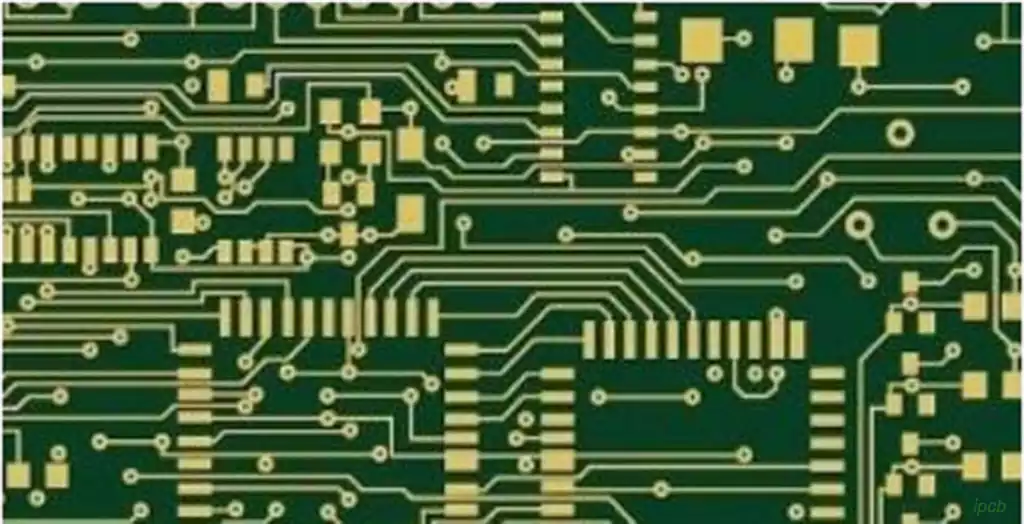
Green oil is the ink coated on the copper foil of the printed circuit board, this layer of ink can cover the accidental conductors other than the pads, to avoid soldering short circuits during use, and to extend the service life of the PCB, which is usually known as solder mask or solder resist film. Colors include green, black, red, blue, yellow, white, and matte colors. Since most PCBs use green soldermask ink, it is often referred to as green oil.
The flat surface of a computer motherboard is the PCB (Printed Circuit Board), which is usually a four- or six-layer board. Relatively speaking, to save money, most low-end motherboards are four-layer boards: a primary signal layer, a ground layer, a power layer, and a secondary signal layer. A six-layer board adds a secondary power layer and an intermediate signal layer, so a six-layer PCB motherboard is more resistant to electromagnetic interference and the motherboard is more stable.