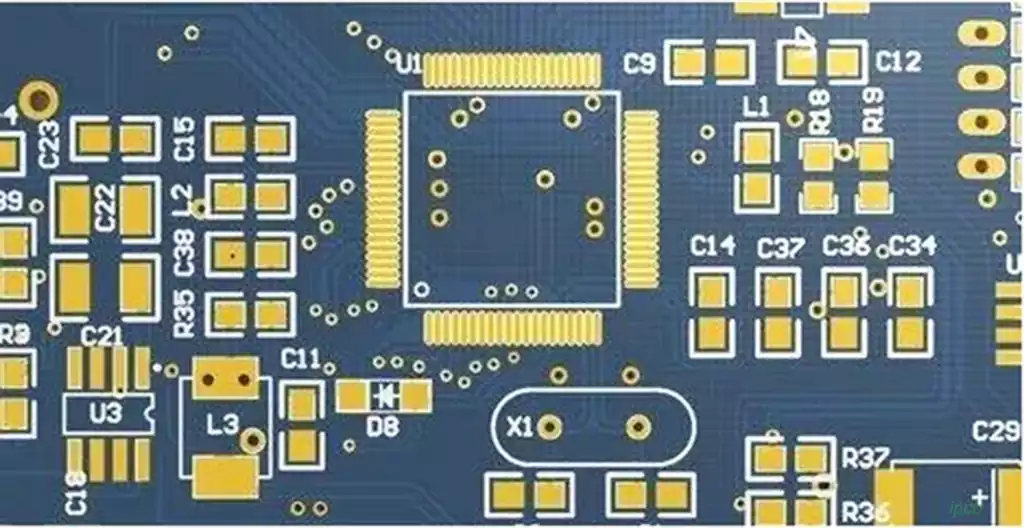
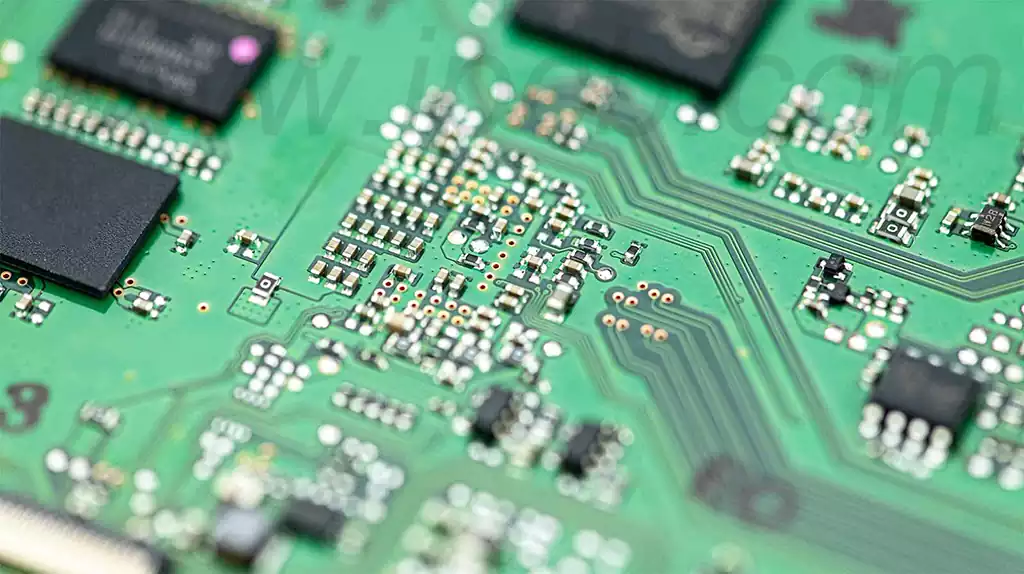
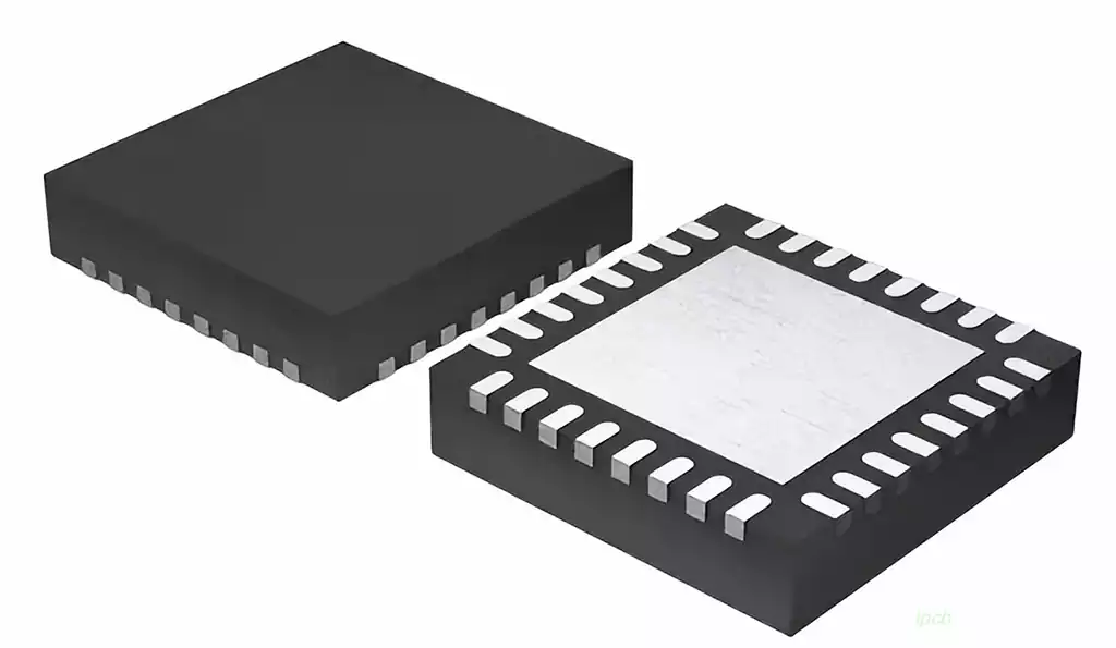
Flip chip packaging technology, also known as FC packaging technology, is an advanced integrated circuit packaging technology. In traditional packaging technology, the chip is encapsulated at the bottom and connected to the package substrate through gold wires. Flip chip technology, on the other hand, flips and mounts the chip directly onto the package substrate, and then connects it using tiny solder joints or conductive glue.
The flip chip packaging process can be subdivided into two processes, FCBGA (Flip Chip Ball Grid Array Package) and Flip Chip Size Package (FCCSP), with Flip Chip Ball Grid Array Package (FCBGA) having a high market share in Flip Chip Packaging (FC). Due to the use of small balls rather than pin welding, this process solves the problem of electromagnetic compatibility and electromagnetic interference, and can withstand higher frequencies; high I/O density, which can effectively reduce the packaging area; the form of chip packaging can make the back of the chip in direct contact with the air, to enhance the chip heat dissipation capability.
Flip chip packaging process mainly includes the following steps:
- Bump: bottom metallization (UBM). This is the starting step of the flip chip packaging process and aims to form a metal layer on the contact points of the chip to facilitate the connection between the chip and the substrate . This process involves the technology of making bumps on the chip surface by sputtering, evaporation, chemical plating or electroplating to form a metallization transition layer (UBM) between the chip pads and the bumps for adhesion and diffusion blocking.
- Formation of chip bumps. This step is to form the connection point, i.e., to make electrodes for the PN junction . The formed bump is a metal ball with uniform body under microscopic view, and the main process includes solder plating. After completing the metallization of the bottom of the bump, the bump for connection is formed through steps such as photolithography and removal of photoresist.
- Wafer Flip Chip. The wafer with the bumps formed is placed onto the substrate by mounting equipment and then heated to connect to the substrate. In this step, the front side of the chip is turned down and connected to the substrate through the bumps to realize the connection between the chip and the substrate.
- Bottom filling. After the flip chip and the substrate are heated to a certain temperature, the filler is injected along the edge of the chip using a syringe containing the filler. Due to the capillary effect of the gap, the filler is drawn in to fill the gap between the chip and the substrate, wrapping the bump. After the filling is completed, the temperature is raised to the curing temperature in sections in an oven and held for a certain period of time until fully cured.
Advantage:
Smaller size: Flip chip technology is more compact than traditional packaging technology and can significantly reduce the size and thickness of electronic products.
Better electrical performance: it can shorten the electrical signal transmission distance, reduce resistance, inductance and other adverse effects, improve the electrical performance of the chip.
Better heat dissipation: Since the chip is in direct contact with the package substrate, it can dissipate heat better and improve the stability and reliability of the chip.
Stronger impact resistance: Flip chip technology in which the chip is tightly coupled with the package substrate has higher impact resistance, which is important for mobile devices and industrial applications and other fields.
Lower cost: it can simplify the packaging process, reduce the required materials and equipment, and lower production costs.
Disadvantages:
Difficult to design: the need to consider the package layout and connection methods at the design stage increases design complexity and challenges. The connection method between the chip and the package substrate needs to be precisely controlled to ensure reliability and stability.
Higher costs: Higher levels of equipment and technology are required in the manufacturing process to ensure accurate mounting and connection of flip chips. This can lead to increased manufacturing costs, especially for smaller production lots.
Thermal management challenges: Flip chips are in direct contact with the package substrate, which makes heat dissipation more difficult. Since the backside of the flip chip is not free to dissipate heat, additional heat dissipation measures are required to keep the temperature of the chip stable, otherwise overheating may occur.
Mechanical Vulnerability: Due to the direct exposure of the chip in this packaging technology, it is susceptible to mechanical stress and physical damage. This can lead to a decrease in the reliability and lifetime of the chip, especially when subjected to forces such as vibration, shock and bending.
Poor repairability: In this type of packaging, the chip is directly attached to the package substrate, making it more difficult to replace or repair the chip in the event of a failure. This can lead to an increase in maintenance costs and may pose a challenge for some application scenarios.
Looking ahead, flip chip packaging technology will continue to lead the innovation in IC packaging, and we need to overcome the challenges of design, cost, and heat dissipation to ensure that its advantages are fully utilized to drive the continued progress of the technology industry.