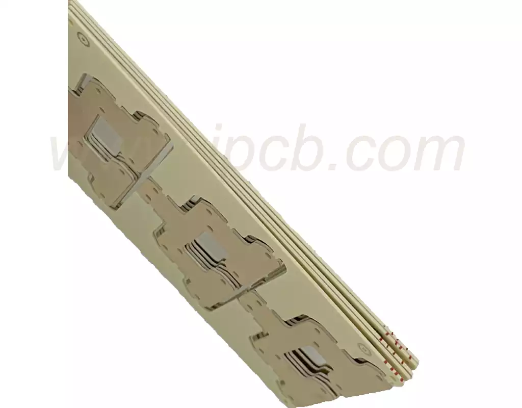
What is LTCC?LTCC is Low temperature cofired ceramic, low temperature cofired ceramic technology. Low temperature cofired ceramic technology (LTCC: low temperature cofired ceramic) is a multilayer circuit made by stacking unfired cast ceramic materials together, with printed interconnect conductors, components, and circuits inside, and sintering the structure into an integrated ceramic multilayer material. LTTC utilizes conventional thick-film dielectric material cast, rather than screen-printed dielectric paste. The raw ceramic tape is cut to the appropriate size, alignment holes and internal cavities are punched, and interconnect vias are formed using laser punching or mechanical drilling. The conductors are screen-printed or photolithographed onto each layer of the ceramic sheet, along with the desired resistors, capacitors and inductors. The layers are then aligned, laminated and co-fired at 850 degrees Celsius. Substrates are assembled and surface mounted utilizing existing thick film circuit manufacturing technology.
LTCC substrate processing is mainly mixed, casting, punching, hole filling, screen printing, stacking, isostatic pressing, sintering and other major processes, the following briefly describes each process technology.
Mixing and casting: organic (mainly composed of polymer binder and dissolved in solution plasticizer) and inorganic (composed of ceramics and glass) components mixed in a certain ratio, grinding and homogenization by ball milling, and then cast on a moving carrier tape (usually polyester film), through a drying zone, remove all the solvents, and through the control of squeegee clearance, casting into the required thickness. The typical thickness tolerance for this process is ±6%.
Perforation: Through holes are formed using mechanical stamping, drilling or laser perforation techniques. Through-holes are small holes (usually 0.1-0.2mm in diameter) punched in the raw ceramic sheet, used in different layers to interconnect circuits. Mold holes are also punched at this stage to aid alignment when stacking wafers; alignment holes are used for automatic alignment when printing conductors and dielectrics.
Printing: The conductor paste is printed and dried using standard thick film printing techniques. Through-hole filling and conductor graphics are dried in chamber or chain ovens at the relevant process temperatures and times. As required, all resistors, capacitors and inductors are printed and dried at this stage.
Through-hole filling: Specially formulated conductor pastes with a high solid particle content are filled into the through-holes using conventional thick film screen printing or stencil extrusion.
Debinding and Sintering: The area between 200-500°C is known as the organic debinding zone (it is recommended to hold the laminations in this zone for a minimum of 60min). The stacks are then co-fired to peak temperature (typically 850°C) in 5-15min. Typical debinding and firing curves for atmosphere firing metallization take 2-10 h. Fired parts are prepared for the post-firing process, e.g. printed conductors and precision resistors on the top surface, and then fired in air. If Cu is used for metallization, the firing must be done in an N2 chain furnace.
Inspection: The circuit is then laser-tuned (if required), tested, sliced, and inspected, and hard-brazed leads or heat sinks (if required) are available in the LTCC package.
Advantages of LTCC technology include:
- High density: High-density circuit patterns and structures can be realized.
- High reliability: Because it is sintered at low temperatures, it can reduce the mismatch between the coefficient of thermal expansion between metals and ceramics, improving product reliability and life.
- Versatility: Multiple functions such as resistors, capacitors and inductors can be integrated on ceramic substrates.
- Precise dimensional control: Fine line pattern and interlayer alignment accuracy can be realized.
- Excellent electrical properties: LTCC materials have good dielectric properties and low loss characteristics, suitable for high-frequency applications.LTCC ceramic chips are widely used in mobile communications, satellite communications, aerospace, automotive electronics and industrial control and other fields.
LTCC technology also has some disadvantages of its own:
- The raw ceramic material is sintered at a high temperature of about 900°. Due to thermal expansion and contraction, the size of the material shrinks when it returns to room temperature, usually by about 10%. In RF circuits, any small change in size may cause a change in circuit performance. Shrinkage control has become a very critical and difficult to control LTCC technology.
2.LTCC technology makes the module integration density increase at the same time, brings the problem of heat concentration, and the ceramic material itself is very poor thermal conductivity, can only be improved through the metallization of the perforation. On the one hand, its heat dissipation effect is still not ideal, especially when the integrated power amplifier is almost unbearable; on the other hand, a large number of perforations will bring the problem of difficult to control the shrinkage rate.
LTCC technology, as an innovation in the field of electronic packaging, has shown great application potential in mobile communications, satellite communications, aerospace and other fields by virtue of its high density, high reliability, multifunctionality, precise dimensional control and excellent electrical properties. However, with the in-depth application of the technology, problems such as dimensional shrinkage and heat dissipation performance of LTCC materials after high-temperature sintering have been gradually exposed.