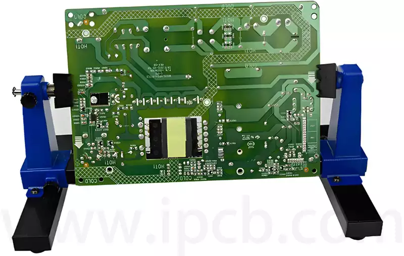
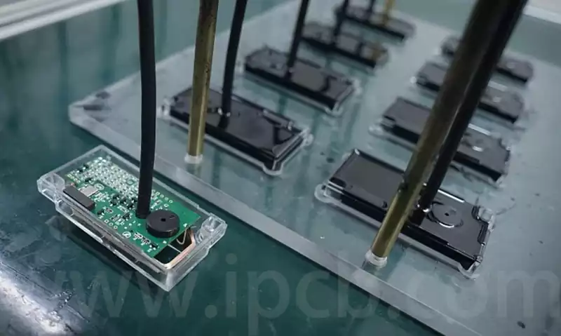
PCB overmolding is a technique that involves coating printed circuit boards (PCBs) with protective polymer resin. This process is designed to protect PCBs from external factors such as humidity, dirt, and temperature fluctuations. During the pcb overmolding process, the polymer resin is injected and cured around the PCB circuitry, forming a tight and secure seal.
This technology can be tailored to meet specific application requirements, ranging from simple coating to complex overmolding methods, including two-shot moulding, insert moulding, and transfer moulding. The success of potting moulding largely depends on the performance of the selected polymer resin.
Through PCB overmolding, the service life and reliability of the circuit board can be significantly enhanced. It helps prevent PCB failures caused by mechanical stress and impact. Additionally, overmolding improves the electrical insulation of the PCB, effectively reducing the risk of short circuits. This technology also allows for customisation of the polymer resin’s colour and texture according to application requirements, enabling personalised product design. This is particularly important in the consumer electronics sector, where user experience and product visual appeal are prioritised.
Minimum thickness for PCB overmolding
The minimum thickness for PCB overmolding depends on the overmoulding material, PCB size, and the required level of protection. Typically, the minimum thickness should ensure that the PCB and its components are adequately protected. To optimise the moulding cycle time, the base material and overmoulding wall thickness should be consistent. In most molding applications, wall thicknesses between 0.060 inches and 0.120 inches (i.e., 1.5 millimetres to 3 millimetres) are feasible.
The thickness of the encapsulation molding also affects the size and weight of electrical equipment. Therefore, the minimum encapsulation moulding thickness must strike a balance between protective properties and equipment size and weight. FR1 PCBs (a commonly used single-layer PCB) typically have thickness restrictions, typically fixed at 1.6 millimetres (0.06 inches). The minimum dielectric layer thickness should not be less than 3 mils. Additionally, the overall thickness of the PCB is directly proportional to thermal resistance.
Other types of PCB boards have various standard thicknesses, including 0.70 mm, 0.80 mm, 0.95 mm, 1.00 mm, 1.27 mm, 1.50 mm, 1.60 mm, 2.00 mm, 2.40 mm, 3.00 mm, 3.20 mm, 3.50 mm, 4.00 mm, and 6.40 mm, among others. During the PCB drilling and copper plating process, the minimum required wall thickness of the holes must be achieved to connect the copper patterns on different layers.
Materials used in PCB overmolding
Thermoplastic plastics
Thermoplastic plastics are materials that can be repeatedly melted, moulded, and remelted. Due to their excellent flexibility, strength, and ease of processing, they are widely used in PCB overmolding
TPU (thermoplastic polyurethane): This material is ideal for applications requiring good shock absorption and wear resistance
TPE (Thermoplastic Elastomer): TPE offers excellent flexibility and is ideal for creating surfaces with a soft tactile feel
PVC (Polyvinyl Chloride): PVC is widely used due to its high cost-effectiveness, moisture resistance, and resistance to mould
ABS (acrylonitrile butadiene styrene): This is a sturdy, lightweight plastic commonly used in consumer electronics
Polypropylene: Polypropylene is lightweight and has good chemical resistance, making it commonly used in industrial applications
Polycarbonate: This material is tough and transparent, making it ideal for applications such as LED covers or enclosed spaces requiring high visibility
Thermosetting plastics
Unlike thermoplastic plastics, thermosetting plastics permanently cure once formed and cannot be reshaped. They are typically used in applications requiring high heat resistance or excellent electrical insulation
Silicone: Silicone is highly flexible and non-toxic, making it ideal for high-temperature or low-temperature environments
PU (polyurethane): Polyurethane offers strong abrasion resistance and mechanical durability
Epoxy resin: Epoxy resin is renowned for its excellent adhesion and high mechanical and chemical resistance
Phenolic resin: This material is strong and heat-resistant, making it ideal for high-reliability applications.
Material Selection Tips
When selecting the most suitable overmoulding material for a product, the following key factors should be considered:
Flexibility Requirements: If the product requires high flexibility, TPE or TPU is the ideal choice
Shell Hardness and Toughness: If a hard and tough shell is required, polycarbonate or ABS is a suitable option
Heat Resistance Considerations: If the operating environment involves high temperatures, silicone or epoxy resin can provide superior heat resistance
Transparent or Light-Sensitive Components: For transparent or light-sensitive components, transparent polycarbonate should be selected
Cost Budget: If cost reduction is the primary objective, PVC can provide good protective performance at a lower cost
Ultimately, the choice of material depends on the specific operating environment of the product, the required performance, and the design objectives. Carefully considering these factors during the planning stage will help ensure that the performance of the moulded PCB fully meets expectations.
Common Design Considerations for PCB overmolding:
Mould Design
Accommodation of Base Parts: The mould design must be able to accommodate and hold the base parts while ensuring that the overmoulding material is evenly distributed over the base parts.
Gate and vent design: Proper gate and vent design is critical for overmoulding. Gates should be located in positions that are easy to remove and do not affect the product’s appearance. The venting system should effectively remove gases from the mould to prevent bubbles and defects.
Draft angle: A suitable angle must be designed to ensure the moulded part can be easily removed from the mould. Different draft angles are required for moulding parts of different shapes and sizes. The draft angle of the mould is determined by the shrinkage rate of the cladding material and the friction coefficient of the mould.
Undercut design: Undercut designs should be avoided on parts whenever possible, as they increase the complexity of mould removal. When undercut designs are necessary, sliders or other complex mould designs should be considered to ensure smooth moulding.
Mould material: Select appropriate mould materials based on the characteristics of the overmoulding material and moulding temperature. For example, for high-temperature moulding materials, tool steel capable of withstanding high temperatures should be chosen.
Material Selection and Compatibility
Adhesion between the substrate and the pcb overmolding material: Ensuring good adhesion between the substrate and the overmolding material is critical. This typically involves a thorough understanding of the chemical and physical properties of both materials to ensure they can bond securely together.
Material selection parameters: When selecting the substrate and coating materials, parameters such as thermal expansion coefficient, surface energy, and wettability should be considered to ensure the formation of a good bonding interface during the moulding process.
Plastic compatibility: Before overmolding, the compatibility of the plastic components with the PCBA should be checked.
Plastic Properties: The plastic used for overmoulding should have good adhesion, expand when heated, prevent current flow, and be resistant to chemicals. The plastic material should also match the thermal distribution of the PCBA to prevent warping or cracking due to thermal stress.
PCB Component Layout
Thickness Uniformity: The thickness of the PCBA should be uniform, with no sharp edges or corners, to prevent stress concentration or trapped air during moulding.
Tight Component Fixation: Components should be thin and securely fixed to the circuit board to minimise variations in moulded cross-sectional thickness.
Vent Holes or Channels: The PCBA should also have sufficient holes or channels to allow air to escape during pcb molding.
High shear-dependent materials: For materials like GLS overmoulded TPE, which have strong shear-dependent viscosity, the mould design and moulding process parameters must be carefully adjusted to ensure optimal flow of the TPE material.
Process Control
Temperature, Pressure, and Time Monitoring: The overmoulding process requires careful monitoring of temperature, pressure, and time to ensure proper curing of the material and adhesion to the substrate. Changes in these process parameters may result in defects such as voids, sink marks, and warping.
Process Optimisation: To shorten production cycles, it is possible to adjust and optimise the process parameters of the moulding process, such as injection speed, pressure, and mould temperature. These measures can improve product quality.
Quality Assurance
Finished Product Inspection: During the overmoulding process, issues can be identified by carefully observing and inspecting the finished product.
Testing and Validation: Testing and validating overmoulded products to ensure they meet performance requirements is crucial. Depending on the application, this may involve testing mechanical, environmental, and electrical components.
Supplier Selection: Collaborating with a reliable and experienced PCB overmoulding supplier is essential to ensure high-quality final results. Manufacturers should review suppliers’ websites, reviews, testimonials, and certifications, and request quotes from multiple suppliers to compare prices, delivery times, minimum order quantities, payment terms, and delivery options. They should also inquire about past work examples and visit their facilities to assess communication skills, response speed, and professionalism.
PCB encapsulation is not suitable for all projects, but it can play a significant role in specific scenarios. When to choose potting:
Harsh operating environments
When products need to operate in harsh environments, potting provides an additional protective layer:
Impact and vibration protection: For equipment frequently exposed to impacts or vibrations, such as industrial machinery, portable tools, or automotive systems, potting effectively protects delicate solder joints and internal components from damage. For example, in the automotive industry, encapsulated PCBs are commonly used in GPS devices and infotainment systems to ensure they function properly under harsh conditions such as high temperatures, vibrations, and dust.
Environmental sealing: Encapsulation forms a comprehensive sealed barrier, effectively preventing moisture, dust, and even corrosive chemicals from entering the PCB, thereby extending the lifespan and performance of equipment in harsh environments such as outdoor settings, factories, or medical facilities. For example, diagnostic tools and portable monitors in the healthcare sector utilise encapsulation to provide sterile, sealed protection and withstand cleaning or disinfection processes.
Space-constrained and integrated design
When products have strict requirements for size and weight, potting moulding can provide a compact, integrated solution.
Space-saving: Potting moulding integrates the PCB and its housing into a streamlined, integrated design without the need for bulky enclosures, making it particularly suitable for devices where every millimetre of space is critical, such as wearable devices, smart sensors, or portable tools.
Simplified design and aesthetics: This technology allows for custom shapes, contours, and ergonomic features, making product designs more appealing. It also enables the addition of custom logos, textures, or ergonomic features without additional assembly steps. For example, consumer electronics such as smartphones and wearable devices often use overmoulding to enhance impact resistance and environmental protection while providing a smooth surface and custom design.
Special Functional Requirements
When products require specific functions such as waterproofing, brand recognition, or unique ergonomic designs, overmoulding is an ideal choice.
Waterproofing and Moisture Resistance: Overmolding creates a sealed barrier around circuit boards, enabling devices to achieve waterproof or moisture-resistant functionality, making it ideal for outdoor or high-humidity applications.
Enhanced User Experience: Overmoulding makes it easier to add waterproofing, custom logos, or soft-touch surfaces, which is particularly useful for consumer products where style, comfort, and brand image are important.
Electrical insulation and signal integrity: PCB overmolding improves a product’s electrical insulation, helping to prevent short circuits and protect against electromagnetic interference (EMI) or radio frequency interference (RFI) that could affect signal integrity, which is especially important for sensitive or high-speed electronic devices.
PCB overmolding technology demonstrates its irreplaceable value across numerous electronic project domains due to its significant advantages. However, when deciding whether to adopt this technology, it is essential to comprehensively consider the project’s specific requirements, cost budget, and technical feasibility, among other factors.