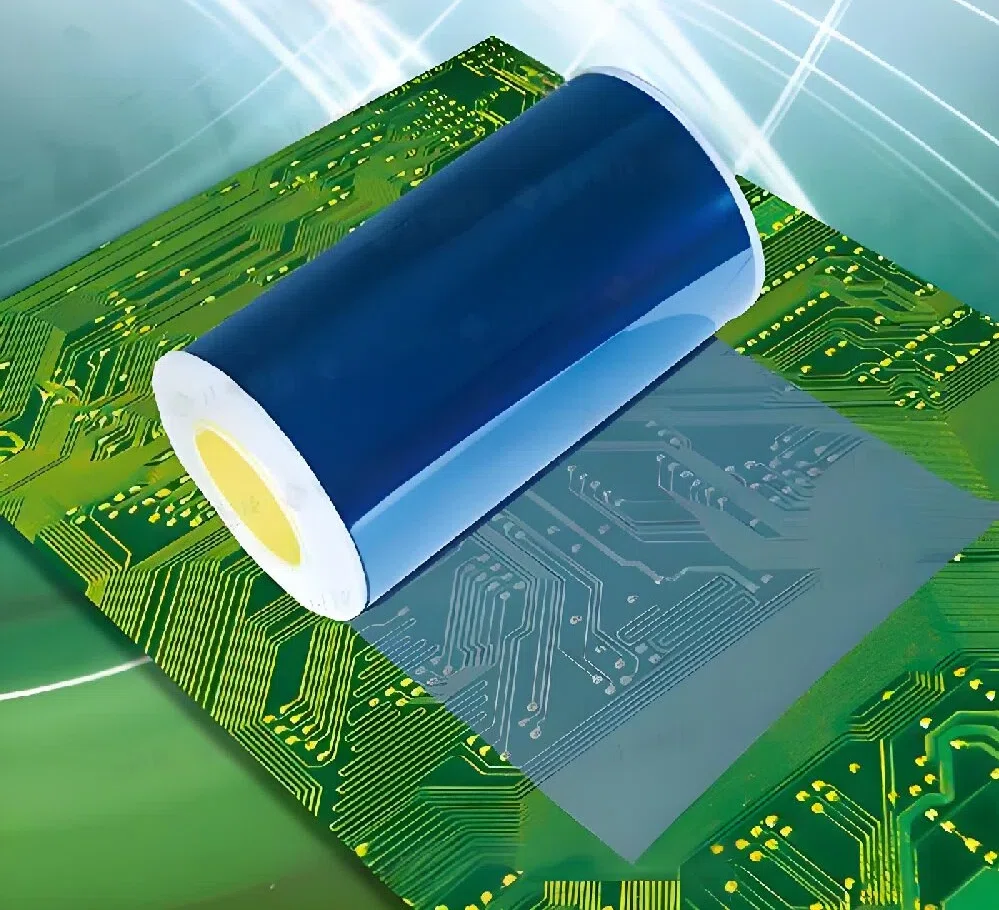
High speed PCB design specifically refers to systems that utilise high speed digital signals to transmit data between components. The boundary between high-speed digital design and simpler circuit boards employing slower digital protocols is not always clear cut.Typically,the key indicator determining whether a system qualifies as ‘high-speed’ is the edge rate (or rise time) of its digital signals. Most digital designs incorporate both high speed (fast edge rate) and low-speed (slow edge rate) digital protocols simultaneously. In the current era of embedded computing and the Internet of Things, most high speed pcb also integrate RF front-ends for wireless communication and networking.
Whilst all designs commence with schematics, the core of high speed PCB design lies in interconnect design, PCB stackup design, and routing. Success in the first two aspects typically paves the way for success in the third. A thorough understanding of high-speed design methodologies and the role of PCB design software is paramount.
High Speed PCB Laminate and Impedance Planning
The PCB laminate created for high speed pcb directly impacts impedance and routing complexity. All PCB laminates incorporate dedicated layers for high-speed signals, power planes, and ground planes. When allocating laminate layers, the following considerations apply:
Board Size and Number of Networks: The physical dimensions of the circuit board and the quantity of networks requiring routing within the PCB layout are critical factors. Larger boards may possess sufficient space for routing throughout the PCB layout without excessive signal layers.
Routing Density: Where network counts are high and board dimensions are constrained, surface layers may lack adequate routing space. In such instances, traces become denser, necessitating additional internal signal layers. Smaller board sizes often inherently demand higher routing density.
Number of interfaces: Depending on bus width (serial or parallel) and board dimensions, routing only one or two interfaces per layer may prove a superior strategy. For high-speed digital interfaces, maintaining all signals on a single layer ensures consistent impedance and skew.
Low-Speed and RF Signals: If the design incorporates low-speed digital signals or RF signals, these may occupy surface layer space otherwise available for high-speed buses or components, potentially necessitating additional internal layers.
Power Integrity: A fundamental aspect of power integrity is employing large power planes and ground planes to meet the voltage levels required by large integrated circuits. These planes should be placed on adjacent layers to ensure high plane capacitance, thereby supporting stable power delivery for decoupling capacitors.
PCB Material Selection, Layer Count, and Thickness Considerations
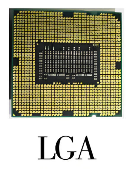
Before designing the PCB stackup, the number of layers required to accommodate all digital signals in the design must be determined. While several methods exist for this, they typically demand mathematical proficiency and experience in high speed PCB design. Beyond the aforementioned layer considerations, large high-speed ICs employing BGA/LGA packaging also influence the required board dimensions. When implementing BGA fan-out, each signal layer typically accommodates two traces, and the total layer count must incorporate power planes and ground planes during stackup construction.

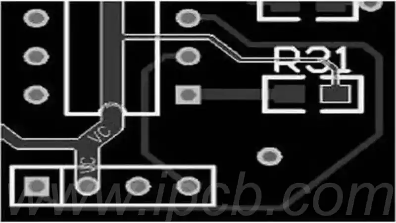
The Importance of High Speed PCB Routing
High speed PCB routing plays a pivotal role in modern electronic devices, serving not merely as a stage in the design process but as a critical determinant of the entire design’s success. In high speed circuit design, this routing demands thorough attention and planning from the outset to ensure the final circuit performance meets expectations. A high-performance circuit meticulously designed on paper becomes unacceptable if its actual performance is significantly compromised due to routing oversights. Therefore, potential issues must be comprehensively considered throughout the design process to enhance performance and shorten design and revision cycles.
Simultaneously, numerous critical aspects demand particular attention during design, notably signal flow direction and power supply configuration and placement. Addressing these issues is especially crucial when considering the impact on operational amplifiers, as even minor oversights can severely compromise circuit performance when these devices operate in high-frequency bands.
The Relationship Between Schematics and Routing
A high-quality schematic does not guarantee excellent routing, but it forms the foundation of an outstanding design. When drafting schematics, the signal flow throughout the entire circuit must be meticulously planned, incorporating as much detailed and useful information as possible. Such design considerations not only aid PCB designers in better understanding circuit requirements but also enhance design and implementation efficiency.
To elevate a standard schematic into an efficient design tool, consider incorporating elements such as waveform descriptions, mechanical information, trace length specifications, and blank area planning. Furthermore, clearly mark components intended for placement on the PCB’s top layer. These enhancements enable other engineers and technicians involved in the design process to grasp the design intent more clearly, thereby improving overall design consistency and efficiency.
Power Optimisation and Bypass Configuration
In high-speed circuits, particularly in operational amplifier applications, a well-designed bypass power configuration can significantly reduce noise. This configuration helps maintain low impedance at the power pins across a wide bandwidth, which is crucial for enhancing the operational amplifier’s performance.
Capacitor Configuration and Selection
When configuring capacitors, their capacitance values and placement must be considered, especially those positioned near the operational amplifier and ground. Through varied combinations of multiple parallel capacitors, lower AC impedance can be achieved across a broad frequency band, thereby delivering improved Power Supply Rejection Ratio (PSRR) performance.
Role and Configuration Examples of Different Capacitance Values
Employing parallel capacitors with varying capacitance values and configurations effectively influences the AC impedance of power pins and the overall circuit stability. Optimising these capacitor arrangements not only reduces noise but also enhances the operational amplifier’s performance when handling high-speed signals.
High speed PCB design constitutes a multidimensional, demanding engineering endeavour requiring meticulous planning across signal integrity, power integrity, and electromagnetic compatibility. Through optimised control of stack-ups, materials, routing, and power delivery, we ensure the exceptional performance and reliability of high-speed circuits.